Cross-Sectional Scanning Tunneling Microscopy
Semiconductor devices are typically fabricated via epitaxial growth on the (001) surface. In order to probe the full set of buried layers using STM, a cross-sectional surface must be produced and it is this surface that the probe tip scans. The situation is clearly shown in Fig. 1, which contrasts planar and cross-sectional STM. Best results are achieved if this surface is unreconstructed, electrically unpinned and atomically flat.14 In this case, the structure of the surface is representative of the structure of the grown layers. In conventional III-V materials such a surface can be produced through an in vacuo cleave to expose a (110) surface. By examining this surface in ultra-high vacuum (UHV), atomic resolution can be achieved12 and reveals an unreconstructed surface with large regions of atomically flat terraces. As well, through carrier injection, photons can be generated in the near-surface region. By collecting these photons, as shown in Fig. 1, the optical properties of the near-surface region (which are representative of those of the bulk) can be spectrally resolved. This technique of scanning the surface and collecting the photons is referred to as scanning tunneling-induced luminescence (STL). On II-VI materials similar qualities of in situ cleaves should be achievable, however in the nitride and group-IV systems such good surfaces are not easily achieved. In the case of Si and Si/SiCGe structures, the crystal can cleave on both (111) and (110) planes15,16, and in vacuum both surfaces reconstruct. The best results have been achieved on hydrogen passivated surfaces.17 The best results for XSTM and related techniques have been obtained for the conventional III-V materials through an in situ (110) cleave. These are described in more detail below. This is followed by a discussion of the less successful results for the group-IV materials.
Conventional III-V Heterostructures:
The nature of the in vacuo (110) cleaved surface of III-V materials is such that the anion (group V) dangling bond becomes a filled surface state in the valence band, and the cation (group III) dangling bond becomes an empty surface state in the conduction band. Thus, depending on tip/sample bias, filled anion-related states or empty cation-related states can be separately imaged.11,19 This situation is shown for GaAs in Fig. 2. (With the exception of this image, all others in this section, are drawn from the research performed by the principal investigator while at IBM Zurich.) The variation of ion size and electro-negativity within group-III or -V elements allows one to determine the ionic species on an atomic scale. This effect provides the atomically resolved chemical sensitivity. An example of this is shown in Fig. 3. In this empty-state cation-related image of InGaAs/AlGaAs quantum wires, Al appears darker20 and In appears lighter than Ga.21 This atomic chemical sensitivity allows the assessment of interface roughness, clustering, segregation, and alloy ordering with atomic resolution. Indeed, these phenomena have already been investigated in various III-V material systems.22-26
The unpinned surface also allows for the probing of bulk energy levels through scanning tunneling spectroscopy (STS).27 In spectroscopic mode, the tip/sample bias voltage is swept, while the current feedback loop is turned off. The valence and conduction band edges can be probed and consequently, doping concentration, doping type, and bandgaps can be determined. (See Ref. 27 for a comprehensive review.) Such spectra executed at different positions across an interface measure the different bandgaps and the pertinent band-offsets as they vary across the interface, with near atomic resolution. STM and STS are also sensitive to defect states within the bandgap, as demonstrated by the real-space imaging of the defect EL2 in GaAs.28 In scanning tunneling potentiometry, a bias is run through the sample, itself, while STS measurements are made; allowing the determination of band edges on a biased device.29 A third aspect of the XSTM technique is the sensitivity to individual near-surface dopants (the top ~10 layers) resulting from their modification of the surface density of states. Zn and Be p-type dopants30,31, as well as Si n-type dopants32 have all been individually observed. Figure 4 shows individual Be dopants in a MBE-grown GaAs buffer layer. The hillock features have a radius that is approximately the Bohr radius and a height ranging up to 0.2 Å.. Most recently Be d-doped layers have been directly observed and it is found that d-layers are not actually confined to one lattice plane, especially, at high dopant densities.33
As mentioned above, in scanning tunneling-induced luminescence (STL) photons generated due to minority carrier injection are collected from the tip/sample region and spectrally resolved. As with cathodoluminescence (CL) the location of the injected current is known (with atomic resolution for STL), while the location of the photon generation is not. However, in STL the injection energies are much lower (about 1 eV c.f. several keV) and the carriers remain confined within quantum structures. Using STL, even densely packed nanostructures can be individually probed, so that their spectral characteristics can be separately measured. This has been well demonstrated in arrays of quantum wires and wells (QWRs and QWs) , where room temperature luminescence was collected from the individual structures.34 Figures 5 and 6 show the STL and STM images taken separately from identically-grown twin samples consisting of an array of stacked quantum wires and wells. The different intensities of the wires is related directly to the efficiencies of the radiative and non-radiative minority-carrier decay channels.34 Figures 5 and 6 represent the first map of the chemical, electronic and photonic properties of a complicated nanostructure with essentially the ultimate resolution possible.
Figure 1: Schematic views of STM arrangement. (a) and (b) show planar and cross-sectional configurations, respectively. Collection of photons from the near-surface region for STL are also shown in (b).
Figure 2: Constant-current STM images acquired at sample voltages of (a) +1.9 and (b) -1.9 V. The surface height is given by a gray scale, ranging from 0 (black) to (a) 0.83 and (b) 0.65 Å?(white). (c) Top view of the surface atoms. Ga and As atoms are represented by solid and open circles, respectively. The rectangle indicates a unit cell whose position is the same in all three figures. (Ref. 12)
Figure 3: STM empty-state cross-sectional image of (a) an In0.12Ga0.88As quantum well embedded in (AlAs)4(GaAs)8 SL barriers (image size 800x220 Å)
and (b) a similarly embedded quantum wire grown on {311}B-side walls (scan size 800x450 Å) Tunneling conditions: sample bias +1.9 V and tunneling current 40 pA. The gray-scale range is 0.6 Å in both images. Individual In atoms appear as atomically sharp white dots, while AlAs regions appear dark. (Ref. 21)
Figure 4: STM image of a (110)-cleaved, 1x1019 cm-3, Be-doped Ga surface. Image displays 31x29 nm of the As sublattice. The relative tip height is given by a gray scale, from 0 (black) to 2.0 Å (white). Nine hillock (dopants) are identified using numbers at the closest point on the perimeter. (Ref. 31)
These include:
The affect of surface roughness on InSb Quantum Well Systems, such as high-mobility electron layers, which display
mobility anisotropy, or multi-quantum wells which show sharp exciton features.
Surface morphology of BaF2/CaF2 Buffer Layers for Growth of PbSe on Si for
Lift-Off applications.
Surface morphology of LPE grown of crack-free PbSe layers on Si(100) using MBE-grown PbSe/BaF2/CaF2 buffer layers.
Eu:CaF2 layers on p-Si(100) grown using Molecular Beam Epitaxy as materials for
Si-based optoelectronics.
Surface roughness of images chemically etched polycrystalline
CdTe solar cell layers.
Publications
Please (Click) on paper to get PDF version.
-
"Be Delta-Doped Layers in GaAs Imaged with Atomic Resolution using STM", M.B.Johnson, P.M.Koenraad, H.W.M.Salemink et al. , Phys. Rev. Lett. 75, 1605 (1995).
-
"Indium distribution in InGaAs quantum wires observed with the STM", M.Pfister, M.B.Johnson, S.F.Alvarado, H.W.M. Salemink, U.Marti, D.Martin, F.Morier-Genoud, and F.K.Reinhart, Appl. Phys. Lett. 67, 1459 (1995).
|
|


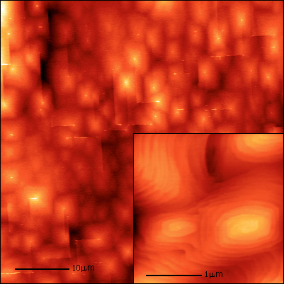 Planar AFM image of InSb-Related Multi-Quantum Well.
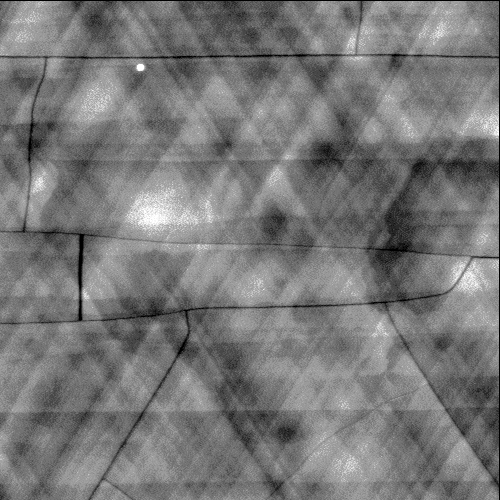 BaF2/CaF2 Buffer Layers for Growth of PbSe on Si