Air SPM of InSb-Related Heterostructures
Recently, we have begun a study of the surface morphologies of InSb quantum well structures. These samples have been prepared in house using MBE techniques.
For InSb based electronic devices, it is important to be able to grow the devices on a GaAs substrate. Therefore, these structures were grown on GaAs with a GaSb buffer layer grown between the substrate and the QW to relax some of the 14% lattice mismatch. The purpose of our study is to investigate the source of the surface morphology seen on InSb quantum wells.
These include:
The affect of surface roughness on InSb Quantum Well Systems, such as high-mobility electron layers, which display
mobility anisotropy, or multi-quantum wells which show sharp exciton features.
AFM Study of High-Electron Mobility InSb Materials
InSb Multiple Quantum Wells
Currently the growth of InSb/AlxIn1-xSb Multiple Quantum Well (MQW)
systems on buffered GaAs substrates incorporate a large number of defects which may
compromise their electronic and optical properties. The defects initiate mainly at
the GaAs/buffer interface and are created to relieve
the strain induced by the mismatch in lattice constants between the growing layers and the
substrate. The defects propagate and
are destroyed as the thickness of the buffer increases and/or is modified
through various compositional changes. The MQW structure, deposited after the buffer
layer, inherits the remaining defects,
mainly in the form of screw or threading dislocations which can be examined at the surface
using Atomic Force Microscopy (AFM). This technique provides us with atomic resolution
of the dislocations along the verticle axis and definitively shows the spiraling staircase
of screw dislocations.
In addition to the standard dislocations, we also see
Oriented Abrupt Steps or OAS's. These steps occur predominately along the
![[1 -1 0]](http://aegir.nhn.ou.edu/~keay/Research/InSb/Images/1bar10.gif) axis, but may also be present along the [110] axis of the material.
Contrary to the screw dislocations the OAS's have steep side wall angles of 5 to 15�
which typically terminates at the peak of a screw dislocation. The OAS could then
significantly alter the quantum well properties. If the MQW
structures follow the surface topology, which is extremely probable, the quantum wells
will become 'pinched' at an OAS, reducing the well spacing, which will effectively change
the electrical and optical properties of the system.
axis, but may also be present along the [110] axis of the material.
Contrary to the screw dislocations the OAS's have steep side wall angles of 5 to 15�
which typically terminates at the peak of a screw dislocation. The OAS could then
significantly alter the quantum well properties. If the MQW
structures follow the surface topology, which is extremely probable, the quantum wells
will become 'pinched' at an OAS, reducing the well spacing, which will effectively change
the electrical and optical properties of the system.
In this work, we are using undoped MQW structures to correlate the structure of these defects,
as viewed by AFM, with the observed optical (exitionic) transitions using Fourier transform infrared
spectroscopy (FTIR). Additional use of X-Ray Diffraction (XRD) in this work helps determine the
amount strain as well as the alloy compostion, x, of the AlxIn1-xSb barrier layers in the system.
Publications
Please (Click) on paper to get PDF version.
-
"Charaterization of InSb Quantum Wells Containing High-Mobility Electron Systems", S.J. Cheung, S.C. Lindstrom, N. Dai, K.J. Goldammer, F. Brown, M.B. Johnson, R.E. Doezema, and M.B. Santos, J. Vac. Sci. Technol. B 17, 1151 (1999).
-
"Electrical Properties of InSb Quantum Wells Remotely-Doped with Si," K.J. Goldammer, W.K. Liu, G.A. Khodaparast, S.C. Lindstrom, M.B. Johnson, R.E. Doezema and M.B. Santos, J. Vac. Sci. Technol. B 16, 1367 (1998).
|
|


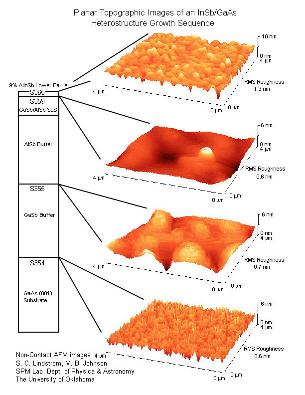 Image profile of QW structure
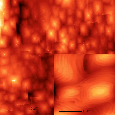 Planar AFM image of InSb-Related Multi-Quantum Well.
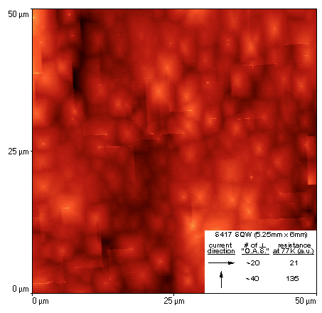 AFM image of single-Quantum Well sample S417 SQW


