
SPM Home
REOS Proposal
Ordering in GaInP
Sample Details
Several samples were grown for XSTM studies.Table 1. Ordered GaInP Samples
|
Run# |
Substrate |
Epilayer |
X-Ray |
PL at 300K |
Morphology |
|
3725 |
GaAs 5o miscut in [01-1], n=2x1018cm-3. |
0.5 mm GaxIn1-xP, Si doped n =1x1017cm-3 |
Mismatch -220ppm, x=48.2% |
688 nm, width 68 nm |
Slip lines |
|
|
GaAs 0o miscut |
|
Mismatch -224ppm, x=47.4% |
676 nm, width 67 nm |
|
|
3727 |
GaAs 5o miscut in [01-1], n=2x1018cm-3. |
0.5 mm GaxIn1-xP, Si doped n=3x1017cm-3 |
Mismatch -310ppm, x=49% |
690 nm, width 69 nm |
No Slip lines |
|
|
GaAs 0o miscut |
|
|
|
|
Results
Only Sample 3725 cleaved well in vacuum. Below are empty and filled state XSTM images of Sample #3725.
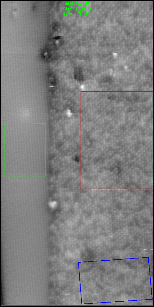 Fig. 1: STM empty-state (group-III related) cross-sectional image of GaInP/ GaAs interface. The scan size is 330x560 A2. Tunneling conditions +3.0 V and tunneling current 10 pA. The gray-scale range is 0.6 A. Individual In atoms appear as atomically sharp dots. Three different areas are delineated by coloured boxes. Green outlines a region of GaAs, Red outlibes a region of defect free GaInP, and Blue outline a second region of GaInP.
With such a high-quality image it is possible to count atoms and hence index the position of atoms throughout the image. This was done relative to the large dopant-like defect above the Green box.
Fig. 1: STM empty-state (group-III related) cross-sectional image of GaInP/ GaAs interface. The scan size is 330x560 A2. Tunneling conditions +3.0 V and tunneling current 10 pA. The gray-scale range is 0.6 A. Individual In atoms appear as atomically sharp dots. Three different areas are delineated by coloured boxes. Green outlines a region of GaAs, Red outlibes a region of defect free GaInP, and Blue outline a second region of GaInP.
With such a high-quality image it is possible to count atoms and hence index the position of atoms throughout the image. This was done relative to the large dopant-like defect above the Green box.
[Click on figure to enlarge]
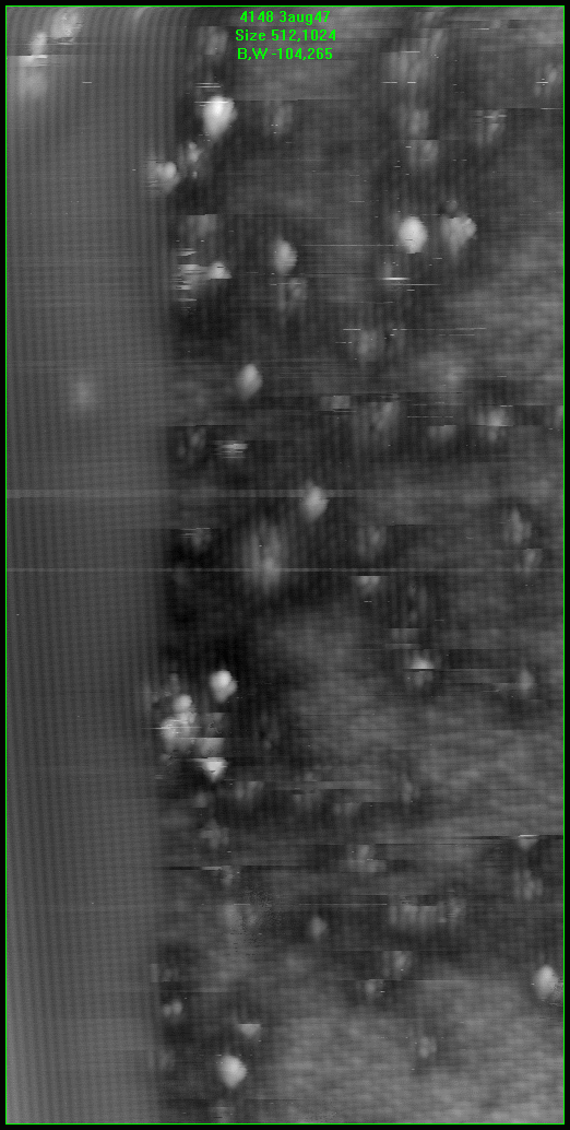 Fig. 2: STM filled-state (group-V related) cross-sectional image of GaInP/ GaAs interface. The scan size is 330x560 A2. Tunneling conditions -2.2 V and tunneling current 10 pA. The gray-scale range is 0.6 A. This scan area is very close to that of the group-III related image of Fig 1. Here too individual In atoms appear as atomically sharp dots. Note the image is not as high-quality as that of the image in Fig. 1 and there are many tip-image type defects observed in the scan. However, there are many large defect-free regions. As with the image in Fig 1. it is possible to count atoms and hence index the position of each atom throughout the image. This was done relative to the same dopant-like used in Fig. 1.
[Click on figure to enlarge]
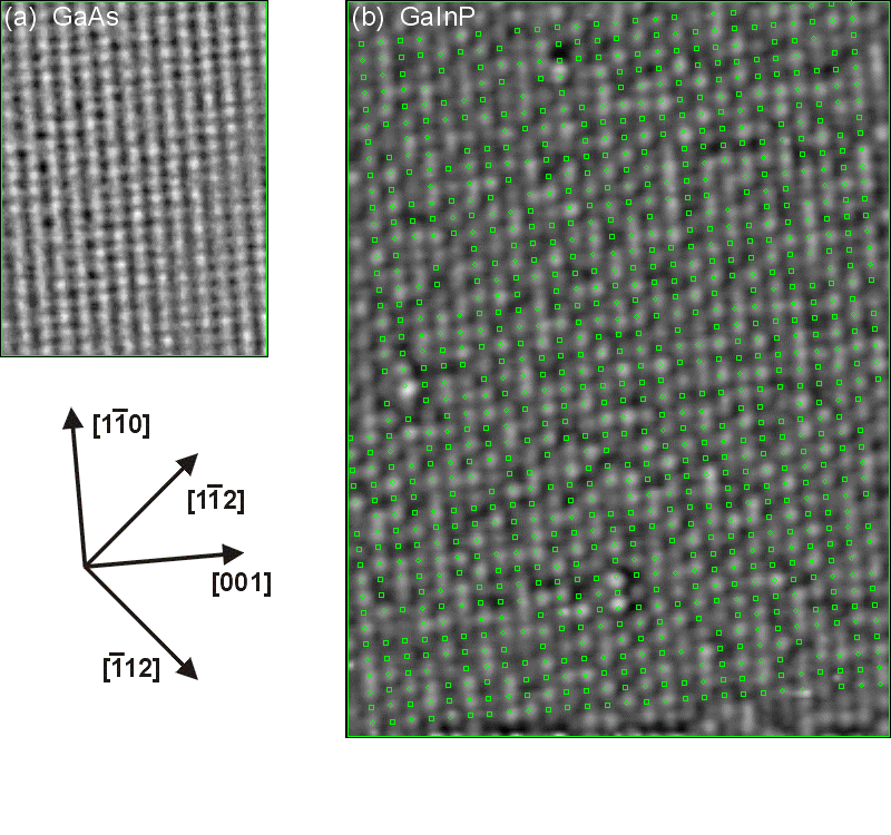 Fig. 3: STM empty-state (group-III related) filtered image of GaAs (a) and GaInP (b).
Both images are low- and high-passed filtered to reduce pixel-to-pixel noise and flatten the image, respectively. Individual atomic positions are marked in both images. (a) shows the area of GaInP surrounded by the Green box in Fig. 1. This is an area of about 14 atoms by 23 atoms. Note the uniform appearance of the atoms. The open rectangle mark the Ga atoms. (b) shows the area of GaInP surrounded by the Red box in Fig. 1. This is an area of about 27 atoms by 45 atoms. Note the bright and dark appearance of the atoms. The open rectangles mark the dark atoms with height less than 2 B/W units as Ga, and open diamonds mark the bright atoms with height greater than 5 B/W units as In.
Fig. 3: STM empty-state (group-III related) filtered image of GaAs (a) and GaInP (b).
Both images are low- and high-passed filtered to reduce pixel-to-pixel noise and flatten the image, respectively. Individual atomic positions are marked in both images. (a) shows the area of GaInP surrounded by the Green box in Fig. 1. This is an area of about 14 atoms by 23 atoms. Note the uniform appearance of the atoms. The open rectangle mark the Ga atoms. (b) shows the area of GaInP surrounded by the Red box in Fig. 1. This is an area of about 27 atoms by 45 atoms. Note the bright and dark appearance of the atoms. The open rectangles mark the dark atoms with height less than 2 B/W units as Ga, and open diamonds mark the bright atoms with height greater than 5 B/W units as In.
[Click on figure to enlarge]
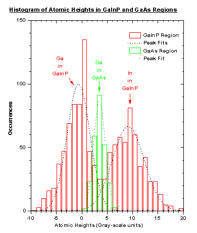 Fig. 4: Histogram of the gray-scale values of Group III atoms.
Red (green) open bars are for the GaInP (GaAs) region. Note the clear bimodal distribution of the GaInP region compared to the single peak of the GaAs region. The FWHM widths of the peaks are: 5.3 for Ga in GaInP, 7.4 for In in GaInP and 2.7 for Ga in GaAs. The wider peaks for the ternary are expected because of the statistical variation of the nearest group III neighbors.
Fig. 4: Histogram of the gray-scale values of Group III atoms.
Red (green) open bars are for the GaInP (GaAs) region. Note the clear bimodal distribution of the GaInP region compared to the single peak of the GaAs region. The FWHM widths of the peaks are: 5.3 for Ga in GaInP, 7.4 for In in GaInP and 2.7 for Ga in GaAs. The wider peaks for the ternary are expected because of the statistical variation of the nearest group III neighbors.
[Click on figure to enlarge]
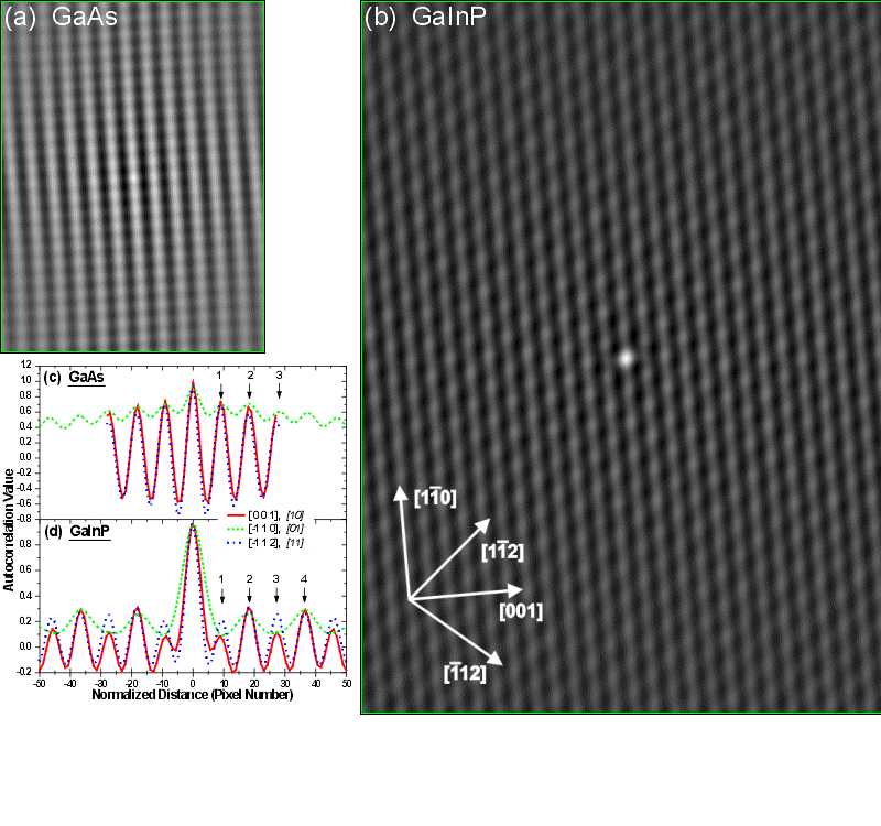 Fig. 5: Autocorrelation images of the GaAs(a) and GaInP (b) regions of Fig. 4 with associated line cuts (c) and (d).
(a) and (b) both show the usual central peak. The GaAs autocorrelation shows an array of periodic peaks indicating the uniform periodic atoms in image 4(b) while the GaInP autocorrelation only shows several peaks close to the central peak. The periodicity of the peaks are very different in the two cases as shown by the line scans drawn through the central peak in the directions repesenting the [ 0 0 1], [-1 1 0], and [-1 1 2] crystallographic directions shown in (c) and (d). The GaAs line scans show peak heights which slowly decrease from the central peak indicating high periodicity in these directions. The GaInP line scans show peak heights strongly alternating in size in the [ 0 0 1] direction but not in the [-1 1 2] direction. This is indicative of a tendency of the In or Ga to order in the [-1 1 2] and [ 1-1 2] directions.
Fig. 5: Autocorrelation images of the GaAs(a) and GaInP (b) regions of Fig. 4 with associated line cuts (c) and (d).
(a) and (b) both show the usual central peak. The GaAs autocorrelation shows an array of periodic peaks indicating the uniform periodic atoms in image 4(b) while the GaInP autocorrelation only shows several peaks close to the central peak. The periodicity of the peaks are very different in the two cases as shown by the line scans drawn through the central peak in the directions repesenting the [ 0 0 1], [-1 1 0], and [-1 1 2] crystallographic directions shown in (c) and (d). The GaAs line scans show peak heights which slowly decrease from the central peak indicating high periodicity in these directions. The GaInP line scans show peak heights strongly alternating in size in the [ 0 0 1] direction but not in the [-1 1 2] direction. This is indicative of a tendency of the In or Ga to order in the [-1 1 2] and [ 1-1 2] directions.
[Click on figure to enlarge]
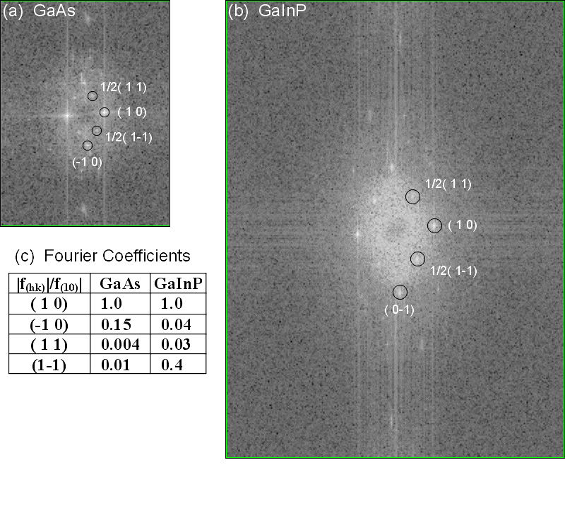 Fig. 6: Fourier Space images of the GaInP (a) and GaAs (b) regions of Fig. 4.
Diffraction spots are labeled according to their 2-D Miller Indices, where [ 1 0] is in the [ 0 0 1] direction and [ 0 1] is in the [ 1 -1 0] direction.
Both images show the expected ( 1 0) and ( 0 1) "diffraction" spots, due to the lines of atoms along the [ 0 1] or [ 1-1 0] and [ 1 0] or [ 0 0 1] directions, respectively.
The GaInP image shows relatively intense 1/2( 1-1) and 1/2( 1 1) spots. The GaAs image also shows these spots, however, they are 10 and 40 times less intense, respectively, and insignificant. In the GaInP image the 1/2( 1-1) spot is about 10 times more intense than the 1/2( 1 1) peak. The 1/2( 1-1) peak is associated with a tendency of In to align in every second line of atoms running in the [ 1 1] or [ 1-1 2] direction, while the 1/2( 1 1) spot is associated with a tendency of In to align in every second line of atoms running in the [-1 1] or [-1 1 2] directions. The fact that the former peak is much more intense indicates that the form of ordering associated with this spot is much more prevalent.
This can be directly observed in the direct-space image of Fig. 4(b) by looking along the [ 1-1 2] and [-1 1 2] directions and noting that there are more lines of In atoms observed in the [ 1-1 2] direction.
Fig. 6: Fourier Space images of the GaInP (a) and GaAs (b) regions of Fig. 4.
Diffraction spots are labeled according to their 2-D Miller Indices, where [ 1 0] is in the [ 0 0 1] direction and [ 0 1] is in the [ 1 -1 0] direction.
Both images show the expected ( 1 0) and ( 0 1) "diffraction" spots, due to the lines of atoms along the [ 0 1] or [ 1-1 0] and [ 1 0] or [ 0 0 1] directions, respectively.
The GaInP image shows relatively intense 1/2( 1-1) and 1/2( 1 1) spots. The GaAs image also shows these spots, however, they are 10 and 40 times less intense, respectively, and insignificant. In the GaInP image the 1/2( 1-1) spot is about 10 times more intense than the 1/2( 1 1) peak. The 1/2( 1-1) peak is associated with a tendency of In to align in every second line of atoms running in the [ 1 1] or [ 1-1 2] direction, while the 1/2( 1 1) spot is associated with a tendency of In to align in every second line of atoms running in the [-1 1] or [-1 1 2] directions. The fact that the former peak is much more intense indicates that the form of ordering associated with this spot is much more prevalent.
This can be directly observed in the direct-space image of Fig. 4(b) by looking along the [ 1-1 2] and [-1 1 2] directions and noting that there are more lines of In atoms observed in the [ 1-1 2] direction.
[Click on figure to enlarge]
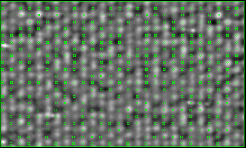 Fig. 7: STM empty-state (group-III related) cross-sectional images of GaInP within the blue outline of Fig. 1. The scan size is 26x20 atoms (??? ??? pixels). The image has been low-pass filtered (averaged) to reduce the noise and high-passed filtered to flatten the image and rotated. The atomic positions are labeled according to the same criteria used in Fig. 3. The open rectangle mark the dark atoms (Ga) while the open diamond marks the bright atoms (In).
[Click on figure to enlarge]
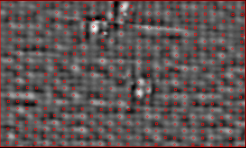 Fig. 8: STM filled-state (group-IV related) cross-sectional images of GaInP within the blue outline of Fig. 1. The scan size is 26x20 atoms (??? ??? pixels). The image has been low-pass filtered (averaged) to reduce the noise and high-passed filtered to flatten the image and rotated. The atomic positions are labeled according to the same criteria used in Fig. 3. The open rectangle mark the dark atoms (Ga) while the open diamond marks the bright atoms (In).
[Click on figure to enlarge]
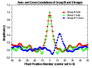 Fig. 9: Line scans across the dominant peaks of the auto- and cross-corelations of the Group-IV related and Group III related images of Fig. 7 and 6, respectively. The line scans are along the x directions. The red and green curves show the autocorrelations of the Group-III and -V related images, respectively. The central peak with amplitude of 1.0 represents direct overlap of the images, while the smaller peaks are due to the atomic periodicity in the images. The blue curve shows the cross-correlation of the group III and V images. The peak with amplitude 0.4 at near pixel 13 indicates a high degree of correlation between the two images with the image positons are offset by about two atoms in the [001] direction (0 atoms in the [ 1-10] direction). This offset appears to be due to variations in the group-V and -III related images of the defect used to align the images.
[Click on figure to enlarge]
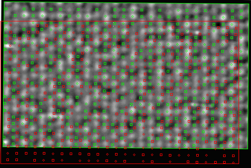 Fig. 10: STM empty-state (Group-III related) cross-sectional images of GaInP, In and Ga in the first and second layers marked. Green squares (diamonds) indicate In (Ga) in the top most layer (from Group-III related image), and red squares (diamonds) mark In (Ga) in the layer below (from Group-V related image). Note the high degree of correlation between the two layers.
[Click on figure to enlarge]
Research | Education | SPM Home
