SPM Lithography
Advanced lithography has been the key technology driver for the semiconductor industry. To sustain the present rate of growth in integration level, the national technology roadmap indicates 100nm technology will ship in 2006, a level where conventional optical lithography will no longer be adequate. As dimensions shrink below 100nm, new resists, processes for making interconnects, and techniques for doping and etching must be found. The development of new pattern transfer processes, and of tools for rapidly prototyping new processes, are essential to the development of next generation lithographies. At OU we are collaborating with a number of groups toward the development of such technologies. Our collaborators include Prof. R.T. Collins of Colorado School of Mines (CSM), Dr. J.-P. Bourgoin of the CEA, FRANCE and Prof. M. Keil of OU.
The collaboration with M. Keil involves the use of his novel atomic fluorine beam to etch extremely anisotropic features in Silicon. Ref. [1] describes recent results in detail. Silicon is found to etch at about 1 mm/min, while fluorinated compounds such as CaF2 and nickel, which forms a non-volatile fluoride, etch very slowly. Most notably using an electron-beam exposed 1 mm wide slot in CaF2 a 1 mm by 120 mm deep trench was etched in Silicon with extremely steep sidewalls and very little undercutting. According to our analysis, similar aspect ratios should be attainable for much narrower trenches, suggesting that this etching technique is ideal for fabricating nanostructures. See [F_etching] for recent results.
The collaboration with R.T. Collins involves his use of near-field scanning optical microscopy (NSOM) to pattern a hydrogen-passivated amorphous Si (a-Si:H) resist layer. Reference [2] below describes recent results in writing features with ~100 nm dimensions. See [a-Silicon] for these results. Currently we are trying to use NSOM patterning and fluorine beam etching to etch features, such as trenches, on the 100 nm scale. Because the fluorine beam etches most usual resists, this requires the use of a process to transfer the NSOM written pattern to film that can act as a mask for the fluorine beam. Currently we are using a nickel film with a wet etch after work by Quate et al. We are investigating NSOM and conventional optical and a-silicon photoresists to write the initial pattern.
The collaboration with J.-P. Bourgoin involves two projects. In the first we demonstrated that fluorinated self-assemble monolayers could resist the fluorine beam up to about 150oC. The second, which is still in progress, involves using e-beam lithography to pattern 100 nm lines in PMMA resists, transfer these to our nickel layer and fluorine etch. This tests whether our Fluorine etching process scales as we propose. See [F_etching] for recent results.
Other in-house work involves using the AFM to "scratch" through ultra-thin PMMA layers and directly wet-etch to transfer this to our fluorine-beam-resistant Ni masks.
Publications
Please (Click) on paper to get PDF version.
-
"Atomic Fluorine Beam Etching of Silicon and Realated Materials," P.R. Larson, K.A. Copeland, G. Dharmasena, R.A. Lasell, M.Keil, and M.B. Johnson, accepted by J. Vac. Sci. Technol. B (1999).
-
"Near-filed scanning optical nanolithography using amorphous silicon resists," M.K. Herndon, R.T. Collins, R.E. Hollingsworth, P.R. Larson, and M.B. Johnson, Appl. Phys. Lett. 74, 141, (1999).
|
|


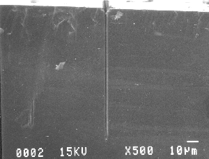 Cross-section of 1mm wide by 120mm deep Trench
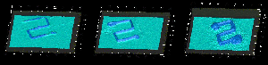 AFM images of NSOM generated patterns
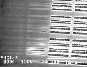 Top down SEM view of fluorine etched trenches in PMGI on Si