Facilities
The Department of Physics and Astronomy at the University of Oklahoma (OU) has
twenty nine faculty members, approximately ten post-doctoral researchers, and
on average fifty graduate students. Four of the seven faculty members in the condensed matter group were hired in the last four years. In 1992, a joint initiative between the stateand the NSF EPSCoR program established the Laboratory for Electronic Properties of Materials (LEPM) at OU. Since 1995, LEPM faculty have been jointly fundedwith investigators at Oklahoma State University and the University of Tulsa through NSF-EPSCoR as the Center for Photonic and Electronic Materials and Devices.
Molecular Beam Epitaxy (MBE) chambers:
Two Varian/Intevac Modular Gen II MBE growth chambers, each with a sample preparation and a sample entry/exit chamber, are located in the Department of Physics and Astronomy. One growth chamber is dedicated to III-V materials (In, Al, Ga, Sb, and As with Si and Be dopants) and the other to fluorides (CaF2 and BaF2),
IV-VI materials (Pb, Se, Te), and rare earth dopants (Eu and Tm).
UHV Analysis Chamber:
Samples from either MBE growth chamber can be transferred under UHV conditions to an adjacent analysis chamber. An x-ray gun, an electron gun, and a hemispherical analyzer manufactured by FISONS Instruments are used for X-ray Photoelectron Spectroscopy (XPS) and Auger Electron Spectroscopy (AES). An argon ion gun for sputtering enables XPS and AES depth profiling of samples. The ion gun is also used for removing oxide layers from InSb substrates.
In SituSTM/AFM Chamber:
A UHV chamber containing a new Omicron Large-Sample STM/AFM (model VT-SPM-DR) will be installed in February 1998. Samples from either MBE growth chamber can be transferred under UHV conditions to this chamber.
Cross-Sectional Scanning Tunneling Microscope:
A cross-sectional STM, used by the MBJ at IBM Zurich, has been donated to the department.
Air Atomic Force and Scanning Tunneling Microscope:
A versatile Topometrix Explorer AFM/STM is used by the PI to characterize semiconductors, polymers, and plastics.
High Resolution X-ray Diffractometer:
A Philips MRD with a four-crystal monochromator is used to characterize MBE samples.
Optical Microscope:
A Nikon OPTIPHOT-66 with Nomarski phase contrast is used to evaluate surface morphology.
Hall Effect Measurement Station:
The carrier density and mobility in MBE samples at room temperature, 77K, and 4.2 K are routinely measured at magnetic fields up to 0.5T.
Deposition Systems:
An Edwards diffusion-pumped two-boat thermal evaporator for contact metalization and a Kurt Lesker turbo-pumped RF- and DC-magnetron sputtering system are used for contact metalization and insulator deposition, respectively.
Equipment available within the Department of Physics and Astronomy
Fourier Transform Infrared Spectrometer:
A Biorad FTS-60A FTIR spectrometer is available to characterize semiconductor structures at room temperature, 77K, and 4.2K.
Low-Temperature Magneto-optical and Magneto-transport Systems:
Quantum transport and optical experiments can be made in an Oxford Instruments 100S dilution refrigerator with a base temperature of ~10mK and a maximum field of 17T provided by a superconducting magnet. Optical excitation is provided by an Edinburgh Instruments far-infrared laser pumped by a CO2 laser.
Instrument and Electronics Shops:
One very valuable resource lies in the department's instrument shop, permanently staffed by three excellent machinists. The instrument and electronics shops provide service without charge.
Computers:
Numerous PCs in the laboratories are used to control experimental apparatus and for data analysis. Most of the PCs are networked together for easy file transfer. Last year, the department acquired an IBM SP2 supercomputer.
Equipment available in other departments
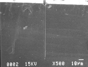
Scanning Electron Microscope
(Microbiology Department): A JEOL JSM880 system, with EDAX equipment, is routinely used to characterize semiconductor heterostructures fabricated by MBE.
Publications
Please (Click) on paper to get PDF version.
-
"Atomic Fluorine Beam Etching of Silicon and Realated Materials," P.R. Larson,
K.A. Copeland, G. Dharmasena, R.A. Lasell, M.Keil, and M.B. Johnson, accepted
by J. Vac. Sci. Technol. B (1999).
|
|


 Cross-section of 1
m
m wide by 120
m
m deep Trench
Cross-section of 1
m
m wide by 120
m
m deep Trench