Air Scanning Probe Microscopy
Air Scanning Probe Microscopy is a simple, elegant, very powerful technique to investigate the topography of a wide variety of samples.
We have used it in collaboration with a wide assortment of groups to assess the growth of various semiconductor crystals.
Our Topometrix Explorer scanning probe microscope (SPM) operates in air or within an controlled air environment.
It can operate as a scanning tunneling microscope (STM) or as and atomic force microscope (AFM).
We use it primarily as an AFM, which allows us to look at non-conductive and conductive samples.
We have found that non-contact operation is the most versatile mode in which to operate.
In this mode, the tip is not in hard contact with the sample, i.e not in the repulsive portion of the force vs. separation curve describing a tip-sample interaction.
Rather we are in the attractive or "van der Waals" portion of the force vs. separation curve.
This non-contact operation is achieved by driving the cantilever, on which the tip is mounted, at one of its resonance frequencies and detecting the amplitude of the response of the tip at this frequency.
Extremely small forces alter the cantilever resonance, which in turn reduces its amplitude. This change in amplitude is easily measured so one can easily measure the small attractive forces between the tip and sample.
Topographic images are made in the usual way by scanning the tip across the sample and maintaining the change in amplitude,caused by the tip-sample force, constant.
This non-contact operation is crucial for soft materials such as polymers and still very useful for softer semiconductors such as InSb and PbSe.
In our measurements we typically use high-aspect ratio Si or silicon nitride tips on high-resonance frequency tips.
The radius of curvature of the tip itself is typically in the 10 to 50 nm range, while the angle of the tip is greater than about 50 o.
Typically our lateral resolution is in the 20 nm range, while our vertical resolution is often below 1 nm.
We routinely measure angles on samples up to 40 to 50o.
We have used such AFM measurements to look a wide variety of samples in order to investigate a
variety of important issues.
These include:
The affect of surface roughness on InSb Quantum Well Systems, such as high-mobility electron layers, which display
mobility anisotropy, or multi-quantum wells which show sharp exciton features.
Surface morphology of BaF2/CaF2 Buffer Layers for Growth of PbSe on Si for
Lift-Off applications.
Surface morphology of LPE grown of crack-free PbSe layers on Si(100) using MBE-grown PbSe/BaF2/CaF2 buffer layers.
Eu:CaF2 layers on p-Si(100) grown using Molecular Beam Epitaxy as materials for
Si-based optoelectronics.
Surface roughness of images chemically etched polycrystalline
CdTe solar cell layers.
Publications
Please (Click) on paper to get PDF version.
-
"Charaterization of InSb Quantum Wells Containing High-Mobility Electron Systems", S.J. Cheung, S.C. Lindstrom, N. Dai, K.J. Goldammer, F. Brown, M.B. Johnson, R.E. Doezema, and M.B. Santos, J. Vac. Sci. Technol. B 17, 1151 (1999).
-
"Electrical Properties of InSb Quantum Wells Remotely-Doped with Si," K.J. Goldammer, W.K. Liu, G.A. Khodaparast, S.C. Lindstrom, M.B. Johnson, R.E. Doezema and M.B. Santos, J. Vac. Sci. Technol. B 16, 1367 (1998).
-
"Eu:CaF2 layers on p-Si(100) grown using Molecular Beam Epitaxy as materials for Si-based optoelectronics," T.Chatterjee, P.J. McCann, X.M. Fang, and M.B. Johnson, J. Vac. Sci. Technol. B 16, 1463 (1998).
-
"LPE growth of crack-free PbSe layers on Si(100) using MBE-grown PbSe/BaF2/CaF2 buffer layers," B.N. Strecker, P.J. McCann, H. Sachar, X.M. Fang, R.J. Hauenstein, M. O'Steen, and M.B. Johnson, J. Elect. Mat. 26, 444-448 (1997)
-
"Sulfur diffusion in polycrystalline thin-film CdTe solar cell," M.H. Aslan, W. Song, J. Tang, D. Mao, R.T. Collins, D.H. Levi, R.K. Ahrenkiel, S.C. Lindstrom, and M.B. Johnson, Mat. Res. Soc. Symp. Proc., 485, 203 (1998).
|
|


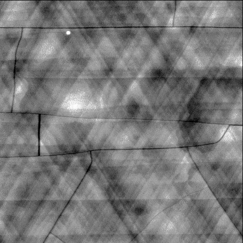
 Planar AFM image of InSb-Related Multi-Quantum Well.
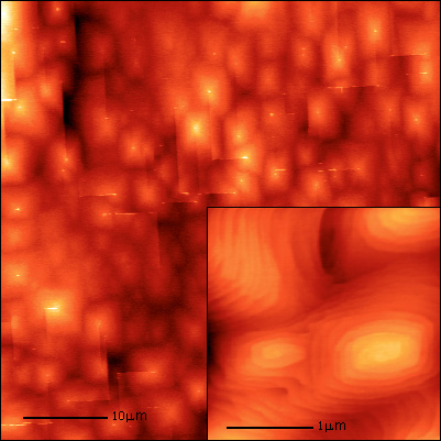
 BaF2/CaF2 Buffer Layers for Growth of PbSe on Si