BaF2/CaF2 Buffer Layers for Growth of PbSe
BaF2 and CaF2 are nearly lattice matched to PbSe and Silicon, respectively. Thus, a BaF2/CaF2 buffer effectively bridges between the large mismatch between PbSe on Si. With such a buffer, high-quality PbSe-related devices can be grown directly on Silicon, which is a benefit because Silicon is much cheaper than the usual substrates for PbSe, and PbSe layers can be incorporated with existing silicon integration technology to produce inexpensive photonic devices. An added benefit resulting from the water solubility of BaF2 is that PbSe films grown on this buffer layer can be bonded to a copper heat sink, removed from the silicon and the exposed PbSe layer can then be used for growth1. This
lift-off
sequence allows PbSe-devices such as lasers to be sandwiched between copper heat-sink layers. Such heat sinking may allow laser operation at higher temperatures.
The purpose of this study was to determine the optimum growth parameters needed to grow high crystalline quality BaF2 on silicon using molecular beam epitaxy (MBE). Based on earlier work2, 200 nm BaF2/20 nm CaF2 buffer layers were grown on Si(111) substrates by MBE and the quality of this BaF2 layer was ascertained. These structures were grown at temperatures in the range of 270-700oC and following the work on CaF2 on Si the effects of rapid thermal annealing (RTA) and thermal soaks (TS) were also studied3. Optical Nomarski Microscopy, Atomic Force Microscopy (AFM) and High-Resolution X-ray diffraction (HRXD) were used to characterize the samples.
AFM and
Nomarski indicate the presence of multiple contributions to the surface roughness. In particular, large crystallites and smaller pyramidal features are observed at both high and low temperatures. At the higher growth temperatures, cracks are visible due to the high thermal mismatch upon cooling. RTA and TS of samples grown at medium temperatures also induce these cracks. Between the cracks, these samples have the smoothest surface morphology of all the layers. Unfortunately, the cracks make the samples useless as buffer layers for PbSe devices. That being the case, the growth at 320oC seems the best in terms of overall surface morphology. At this temperature, shallow pyramidal features are observed with roughness of 10 nm RMS.
HRXDsupports the high quality of the BaF2 grown at 320oC and also indicates the presence of residual stress in the samples grown or annealed at higher temperatures due to the large thermal mismatch upon cool down.
The efforts to improve the surface morphology with RTA alone or with TS proved to be unsuccessful, unlike in the more simple case of CaF2. There, RTA was used to improve surface morphology and TS was used to reduce the affect of the large stress induced due to the large thermal expansion difference between the material. In the case of BaF2, the large lattice mismatch in addition to the large thermal mismatch proved to be too much for the lattice to incorporate, and the formation of cracks was observed to relieve the stress. In summary, the optimal growth temperature for the formation of high quality BaF2/CaF2 on Si(111) appears to be 320oC. In general, these samples showed the smoothest surface morphology (as indicated by AFM and Normarski) and the highest crystalline quality (as indicated by HXRD).
References
- H. Z. Wu, X. M. Fang, R. Salas, Jr., D. McAlister, P. J. McCann, "MBE Growth of BaF2-coated Si(111) and Observation of the PbSe Growth Interface," 17th North American Conference on Molecular Beam Epitaxy, (1998).
- S. Blunier, H. Zogg, C. Maissen, A. N. Tiwari, R. M. Overney, H. Haefke, P. A. Buffat, and G. Kostorz, Phys. Rev. Lett. 68, 3590 (1992).
- Loren Pfeiffer, Julia M. Phillips, T. P. Smith, III, W. M. Augustyniak, and K. W. West, Appl. Phys. Lett. 46, 947 (1985).
|
|


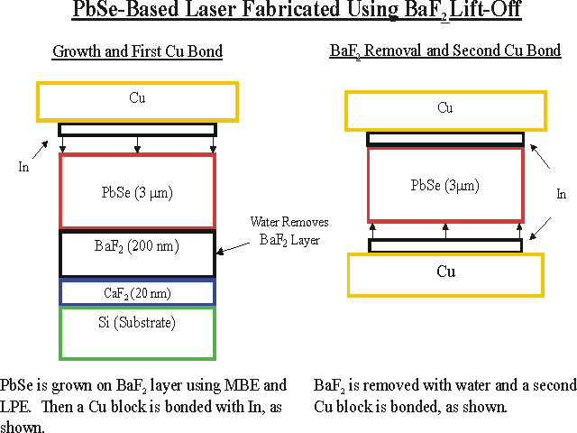 Lift-Off Procedure
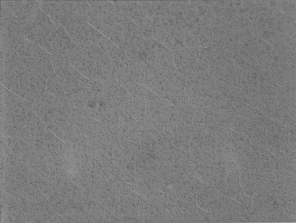 Microscopy of the Layers grown at Different T.
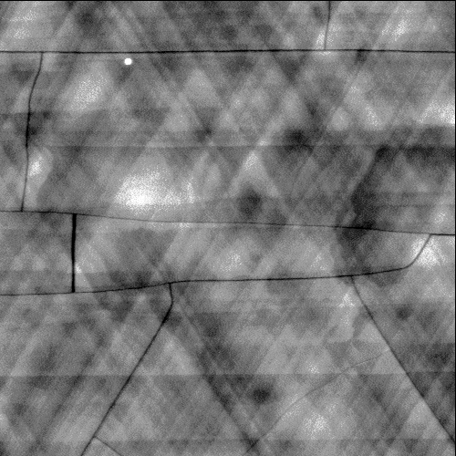 Microscopy of the Layers with Rapid Thermal Anneal.
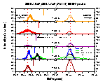 X-Ray spectra
 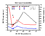 Roughness and Crystalline Quality