NSOM Lithography
Near�field scanning optical microscopy (NSOM) patterning of hydrogenated amorphous silicon (a�Si:H) has been explored. Our sample preparation technique produces films that are stable over several days. The etching process used is highly selective, allowing the unexposed a�Si:H to be completely removed while patterns with line heights equal to the original film thickness remain in exposed regions.
We are able to generate patterns with and without the use of light.
We have found that the probe dither amplitude greatly affects the linewidth and height of patterns generated without light. We also find that the exposure required for the NSOM to optically generate patterns agrees with threshold dosages determined by far�field exposure studies.
Feature sizes of approximately 100 nm, comparable to the probe diameter, were obtained.
(Abstract from paper listed below.)
Our collaborators at the Colorado School of Mines are researching a novel form of proximal probe lithography using near field optical microscopy (NSOM) to generate patterns on amorphous Si on the order of 100 nm. Basically, they take a tapered fiber optic cable with an opening of roughly 100 nm and dither it above the surface (~4-20 nm) of an amorphous Si substrate. They have found that they can generate a pattern with this technique with or without light shining down the probe (i.e. the tapered fiber optic cable). Also, they have found that the dither amplitude affects the linewidth of their pattern. The area where the probe is scanning causes the hydrogen on the Si surface to desorb leaving behind Si which then oxidizes. They can then etch the sample in a dry plasma etching system set up so that the chemistry of the plasma has a high selectivity of etching amorphous silicon over silicon dioxide. In this way the pattern is transferred into the substrate.
This technique could have useful applications in the fabrication of microelectronic circuits.
For our part, we received their patterned samples and imaged them with our ambient atomic force microscope (AFM) to analyze the size of their patterned features. Because of the small size of the patterns, finding them and imaging them posed a significant challenge.
[ Figure 1] below shows
three AFM images of the patterns generated by the CSM group. The image on the left shows a pattern generated with no light. The middle and right images were generated with light with the image on the right having a higher dither amplitude.
[ Figure 2] shows a
closeup AFM image of the pattern generated with no light.
The linescan below the image shows the line width and height.
Publications
Please (Click) on paper to get PDF version.
-
"Near-filed scanning optical nanolithography using amorphous silicon resists," M.K. Herndon, R.T. Collins, R.E. Hollingsworth, P.R. Larson, and M.B. Johnson, Appl. Phys. Lett. 74, 141, (1999).
|
|


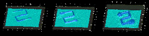 Fig. 1: AFM images of NSOM generated patterns.
 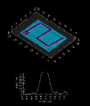 Fig. 2: AFM image of NSOM generated pattern.