Fabrication of High Aspect Ratio Nanostructures in Si Using an Atomic Fluorine Beam
The ability to etch highly anisotropic features in silicon has been, and will continue to be, a crucial requirement for the size reduction of devices in integrated circuits. Currently, dry etching techniques such as plasma etching and reactive ion etching are used to transfer patterns into device substrates. These techniques have had remarkable success in fabricating highly anisotropic features, but they suffer from several disadvantages affecting their ability to etch such structures on a still smaller scale. These disadvantages include: substrate damage due to charging and ion bombardment, feature-size dependence on the etch rate, and undercutting due to sidewall charging and scattering of reactive species. Recently, atomic beam techniques have been developed1 that have the ability to etch anisotropic features into substrates2. With their relatively simple chemistry and use of low energy neutral atoms, these techniques do not suffer from several of the disadvantages listed above.
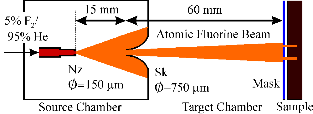
We are researching an application of an intense
atomic fluorine beam to rapidly etch
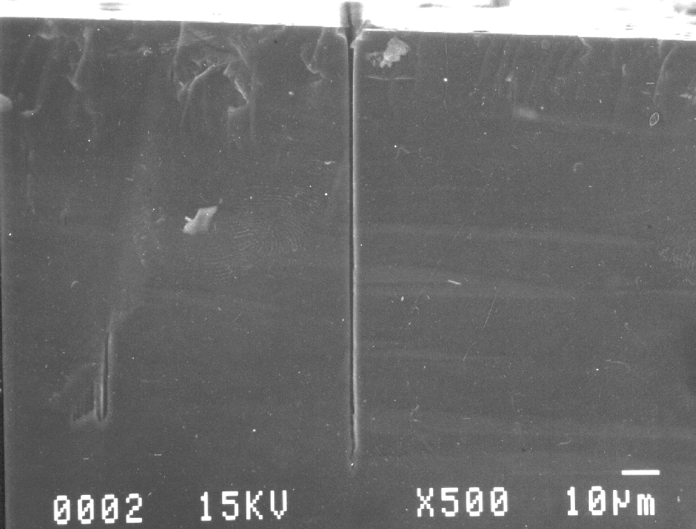
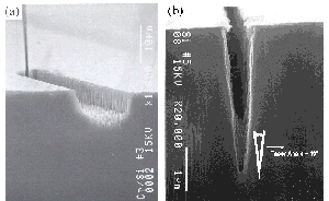
silicon and related materials. In addition, we conduct experiments that utilize the inherently collimated nature of atomic beams to fabricate extremely anisotropic high aspect ratio trenches in Si. The figure below shows a cross-sectional SEM view of a 1 mm-wide, 120 mm-deep
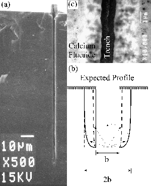
trench in Si(100). This trench is extremely anisotropic, with an aspect ratio of about 120:1 and a sidewall slope of about 1000:1 over nearly the entire depth. To the best of our knowledge, these aspect ratios and sidewall slopes are comparable to or higher than those currently achievable by reactive ion etching. Trenches of the width and depth demonstrated here may be useful to micro electro-mechanical systems (MEMS) applications, as well as isolation trenches in integrated circuits.
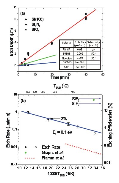
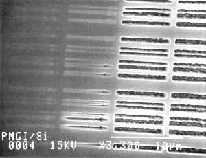
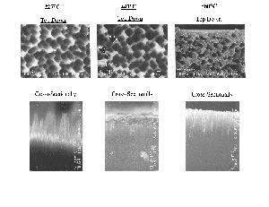
We are now in the process of scaling the size of these trenches down to the nanoscale regime. In particular, it should be possible to maintain high aspect ratios of 100 or greater while shrinking the width of these trenches to 100 nm or less. However, we have found that the role of the substrate temperature of the samples while etching greatly affects the trench profiles. In particular, the higher the temperature, the steeper the sidewall slopes. This presents a problem in finding a good high temperature resist capable of withstanding long term exposure to the fluorine beam. Currently, we have fabricated roughly 100 nm wide trenches using standard organic resists, but were unable to etch deep trenches due to the inability of the resists to withstand the fluorine beam. Next, we fabricated roughly 300 nm wide trenches with aspect ratios of around 10 using a thin layer of Cr as our resist. However, we have found that Cr also etches when exposed to the fluorine beam, which again limited the depth we could etch into the Si. We are now researching the use of Ni as our fluorine resistant mask. Initial research into this area seems promising but no results have yet been produced.
[Link to paper for details.]
References
"Atomic Fluorine Beam Etching of Silicon and Related Materials," P.R. Larson, K.A. Copeland, G. Dharmasena, R.A. Lasell, M.Keil, and M.B. Johnson, accepted by J. Vac. Sci. Technol. B (1999).
- G. Dharmasena, K. Copeland, J. H. Young, R. A. Lasell, T. R. Phillips, G. A. Parker, and M. Keil, J. Phys. Chem. A 101, 6429 (1997); M. Keil, J. H. Young, and K. Copeland, "Method and Apparatus for Etching Surfaces with Atomic Fluorine" U. S. Patent #5,597,495.
- K. P. Giapis, T. A. Moore, and T. K. Minton, J. Vac. Sci. Technol. A 13, 959 (1995).
- L. Flamm, V. M. Donnelly, and J. A. Mucha, J. Appl. Phys. 52(5), 3633 (1981).
- Y. Hirose, S. Horng, A. Kahn, C. Wrenn, and R. Pfeffer, J. Vac. Sci. Technol. A 10(4), 960 (1992).
- G. Nassiopoulos, S. Grigoropoulos, E. Gogolides, and D. Papadimitriou, Appl. Phys. Lett. 66(9), 1114 (1995).
- J. K. Bhardwaj, H. Ashraf, Proceedings of the SPIE 2639, 224 (1995).
- S. Hwang, C. M. Anderson, M. J. Gordon, T. A. Moore, T. K. Minton, and K. P. Giapis, Phys. Rev. Lett. 77, 3049 (1996).
|
|


 Cross-section of 1mm wide by 120mm deep Trench
 Atomic Fluorine Beam Source
 Open Area Etch Results
 High Aspect Ratio Trenches
 Organic Resist Results
 Cr Resist Results
 Temperature Effects