 Fig. 5 Chrome Resist Results.
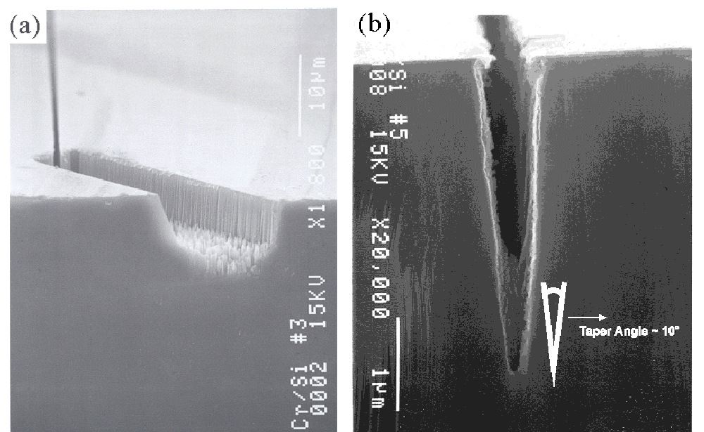
(a) SEM view of fluorine etched trench in Si fabricated using a double layer resist technique. The sample consisted of 60 nm e-beam patterned PMMA on 50 nm evaporated Cr. The pattern was transferred to the Cr layer by means of a Cr wet etch. The sample was then etched in the fluorine beam for 17 minutes at 250oC. (b) Cross-sectional SEM picture of fluorine etched trench in Si. The sample was fabricated in the same manner as (a). The resulting trench is 300 nm wide and 3.4 mm deep. Note the sidewall taper of about 10o.
Our experience with organic photoresists indicated that we needed to find another more suitable high temperature fluorine resist. With this idea in mind, we attempted a double resist transfer technique using e-beam patterned photoresists to define the pattern, with an underlying Cr layer providing the mask to the fluorine.
The patterned was transferred from the photoresist to the Cr layer by means of a Cr wet etch, and then the sample was exposed to the fluorine beam. Figure 5 (a) and (b) shows SEM views of trenches fabricated in this way. The samples consisted of ~ 60 nm e-beam exposed PMMA on ~ 50 nm evaporated Cr on Si(100). The sample in Figure 5 (b) was fluorine etched for 17 minutes at a substrate temperature of 250oC.
The width of the trench is about 300 nm and the depth is roughly 3.4 mm, giving it an aspect ratio of around 11. Unfortunately, the Cr did not work as well as we hoped, as it etched at a rate of about 8 nm/min at 250oC.
Once again, this limited the ultimate depth we could etch the Si.