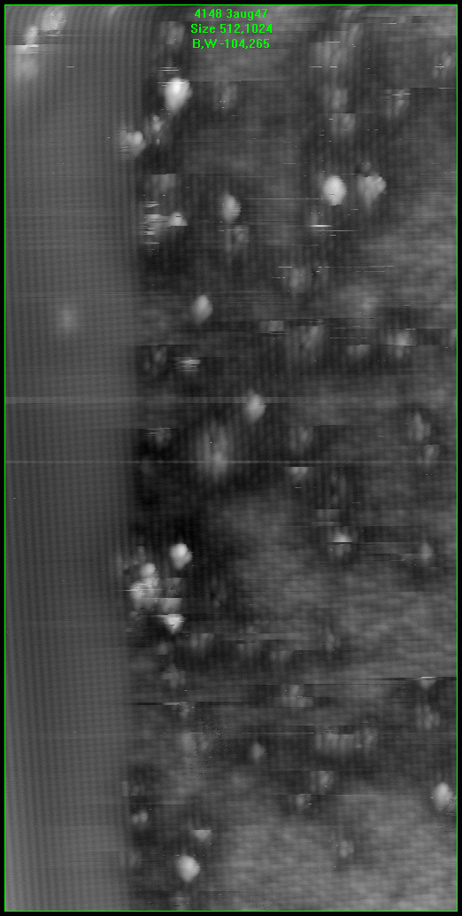
 Fig. 2: STM filled-state (group-IV related) cross-sectional image of GaInP/ GaAs interface. The scan size is 330x560 A2. Tunneling conditions -2.2 V and tunneling current 10 pA. The gray-scale range is 0.6 A. This scan area is very close to that of the group-III related image of Fig 1. Here too individual In atoms appear as atomically sharp dots. Note the image is not as high-quality as that of the image in Fig. 1 and there are many tip-image type defects observed in the scan. However, there are many large defect-free regions. As with the image in Fig 1. it is possible to count atoms and hence index the position of each atom throughout the image. This was done relative to the same dopant-like used in Fig. 1.
[Click on figure to enlarge]
 Fig. 2: STM filled-state (group-IV related) cross-sectional image of GaInP/ GaAs interface. The scan size is 330x560 A2. Tunneling conditions -2.2 V and tunneling current 10 pA. The gray-scale range is 0.6 A. This scan area is very close to that of the group-III related image of Fig 1. Here too individual In atoms appear as atomically sharp dots. Note the image is not as high-quality as that of the image in Fig. 1 and there are many tip-image type defects observed in the scan. However, there are many large defect-free regions. As with the image in Fig 1. it is possible to count atoms and hence index the position of each atom throughout the image. This was done relative to the same dopant-like used in Fig. 1.