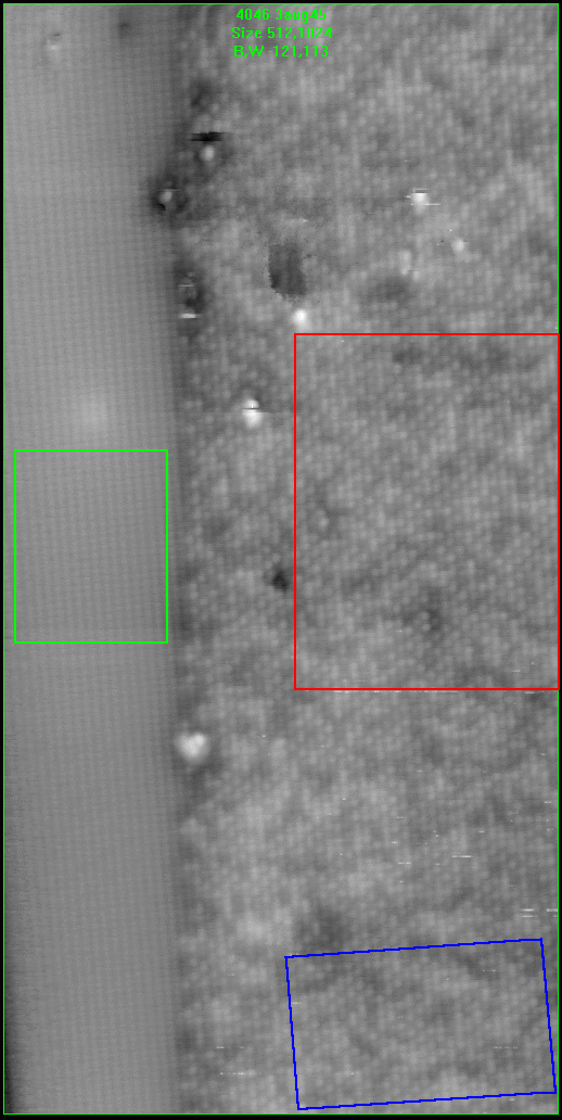
 Fig. 1: STM empty-state (group-III related) cross-sectional image of GaInP/ GaAs interface. The scan size is 330x560 A2. Tunneling conditions +3.0 V and tunneling current 10 pA. The gray-scale range is 0.6 A. Individual In atoms appear as atomically sharp dots. Three different areas are delineated by coloured boxes. Green outlines a region of GaAs, Red outlibes a region of defect free GaInP, and Blue outline a second region of GaInP.
With such a high-quality image it is possible to count atoms and hence index the position of atoms throughout the image. This was done relative to the large dopant-like defect above the Green box.
Fig. 1: STM empty-state (group-III related) cross-sectional image of GaInP/ GaAs interface. The scan size is 330x560 A2. Tunneling conditions +3.0 V and tunneling current 10 pA. The gray-scale range is 0.6 A. Individual In atoms appear as atomically sharp dots. Three different areas are delineated by coloured boxes. Green outlines a region of GaAs, Red outlibes a region of defect free GaInP, and Blue outline a second region of GaInP.
With such a high-quality image it is possible to count atoms and hence index the position of atoms throughout the image. This was done relative to the large dopant-like defect above the Green box.
[Click on figure to enlarge]