Getting started with the Xilinx Project Navigator and the NEXYS Digilab board.
Installation: By far the easiest way to install this software is to go to use the following link. You will need to register, but it is free. This is serious professional software, not some watered down educational junk. Be warned the full package is nearly 16.7 gigabyte installed!
For instructions visit: http://www.nhn.ou.edu/~bumm/ELAB/DigiLab_software.html
To start:
open Xilinx
Project Navigator
select a new project
select a new project name and directory
choose 'Schematic' as the top level module type
next>
Evaluation Development Board: (default) None Specified
product category: (default) All
family: Spartan3
device: XC3S200
package : FT256
speed: -4
top-level source type: Schematic (grayed)
synthesis tool: (default) XST (VHDL/Verilog)
simulator: (default) ISim (VHDL/Verilog)
preferred language: (default) VHDL
Property Specification in Project File: (default) Store non-default values only
Manual Compile Order: (default) unchecked
VHDL Source Analysis Standard: VHDL-93
Enable Message Filtering: (default) unchecked
next>
A summary of the setting is displayed Click OK to complete.
There are some differences of behavior between software versions in the next step.
In the top left window in the "Design" window ("Design" tab selected, bottom left). You will see the the name of your chip "xc3s200-4ft256" as the first item below the name of your project in the project hierarchy. Expand this item. If the message says "Empty View" then you need to add a "source" to your project. Some versions/settings of the software create this intital source schematic for you.
Add a source schematic with the "New Source Wizard" (if needed). There are two ways to open the New Source Wizard. 1) Right click on the chip name and select "New Source" OR 2) in the "Project" drop down in the top navigation bar, select Select "New Source". The "New Source Wizard" window will open. Select source type = Schematic and then provide a name for the schematic. Accept the default directory. This schematic will be placed in the directory of the current project by default. Click "next" and the summary appears. Check that this is what you intend. If all is well, click finish. You will now see your schematic in the hierarchy below your chip.
Now you can
draw the schematic
place devices
wire devices
assign I/O
check the schematic for errors by clicking on the "check mark"
save the schematic
return to Xilinx Project Navigator
Test the schematic design for problems. With the *.sch file highlighted in the "sources" window, go to the "processes" window and right click on "check design rules" under "design utilities" (you may need to expand this item) from the pop-up menu select "run" or "rerun." Errors will be inducted in the "console" window at the bottom.
Next assign the I/O port to the XS3CS200 package pins. You will need the table of the pin-outs and functions to do this. With the *.sch file highlighted in the "sources" window, go to the "processes" window and right click on "floorplan Area/IO/Logic (PlanAhead)" under "user constraints" (you may need to expand this item) from the pop-up menu select "run" or "rerun." Double clicking will also work. If this is the first time to assign pins in this project you will get a message "This process requires that an Implementation Constraint File (UCF) be added..." click yes to create one. A new window "PlanAhead" will open with a diagram of the XS3CS200 among other windows. The important part is the table at the bottom "showing the I/O ports named as in your schematic and the "I/O Port Properties" window above it. Select the port to assign in the "I/O Ports Window". You may need to expand "all ports" and "scalar ports". The selected port will appear in the I/O Ports Properties window. Enter the pin assignment in the "site" box. Click the "apply" button that appears. The I/O ports table will update with the new pin assignment. After you have assigned all your pins, chose "save floorplan" from the "file" drop down menu.
UCF files are simple text files. You may find it easier to manipulate them using a text editor once you have a UCF file generated that you can use as a template. Be careful. The format and syntax are rigid. So a typo will probably cause your design to fail.
You can now generate the programming file. With the *.sch file highlighted in the "sources" window, go to the "processes" window and right click on "Generate Programming File" under "Implement Design" and select "run" or "rerun". When this has completed, the Console windows should say: Process "Generate Programming File" completed successfully. The Design Summary Window contains a summary of the result, along with lots of other statistics. If all goes well, a green check mark will appear beside the "Implement Designs" and "Generate Programming File". You should have no errors. Errors are fatal for the program file generation process. Warnings are alerts that something might be wrong with your design (e.g. ports not assigned to pins), but are not fatal.
If you do not have a USB port. Programming using the parallel port and the JTAG cable. Refer to the Nexys and Adept documentation.
Programming the Nexys board using the USB cable. Open "Adept" the program found in the nested program group Digilent > Adept > Adept.
Before attempting to program using the USB cable, the board must be set up properly. 1) Set the shunt on J4 to USB, this enables the Nexys to draw power form the USB port. 2) Set the shunt on J6 to bridge TD0 and TD1. 3) Set the shunt on JP3 to "flash mode" (bridge the 2 pins on the side marked "flash"). Connect the board to your computer using the USB cable and turn the power switch on the Nexys board to the "on" position". The red power LED (LD-P) should light.
Start "Adept" and a windows opens. Adept should autodetect the USB device (this is the default), e.g. Connect: "Onboard USB", product: "Nexys - 200". If it doesn't, make sure the the power switch on your Nexys board is in the "on" position.
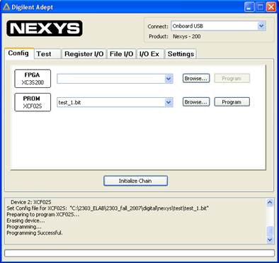
To program your board, open the "Config" tab. In order to proceed, you must have already generated the .bit programming file in the Xilinx Project Navigator. The .bit file is for the PROM. Click on "Browse", then navigate to the .bit file you have created, which will be in your Xilinx project directory. After selecting the file, it will appear in the drop-down box as shown in the example. Click on the "Program" button at the right to program the Nexys board. Your program will begin running immediately after programming is complete.
Working with Modules. You can add a circuit you have already made to another project in the form of a module. To add the module to an existing schematic, right click on the schematic file (*.sch) and select "add source" or "add copy of source". Then select the appropriate source file that you wish to use as the module. If the circuit you would like to include is a schematic file (*.sch) choose that. If you want to include the hex2led_decoder I have posted for you, you need to select the *.vhd file. Once added to the project, you may need to generate the symbol for that module. To do this, highlight the source you have just added and then in the "Processes" window select >Design Utilities>Create Schematic Symbol. After you have done this, the symbol for your module will be available in the schematic capture editor. It will be assigned to a category named by the directory in which it resides.
Editing the pin order in your module. When you add the modules symbol to the schematic, you will see that the module is represented by a rectangle with inputs and outputs. The order of the ports is assigned automatically and may be inconvenient. You can change the order that the ports appear on the symbol. To edit the symbol, open the *.sch source file for the module in the schematic capture editor, then select "symbol wizard" from the "tools" menu. The "Symbol Wizard" window opens. Under "pin name source" select "using schematic" then select the appropriate module name from the list. Click next to view a table of the input/output pins and the order of the pins. Change the order of the pins as desired by clicking on the cell in the "order" column. Once your changes have been made, click next to see other options. Clicking next again will show you a preview of you symbol. Use the back button to make changes as desired. When you are finished, click the "finish" button". You will be prompted to overwrite the *sym files that you have changed. Accept this if you are generally a happy person. If you have already included the symbol that you just changed into a schematic, you must face the repercussions of your actions. Open the schematic and you will get window showing "obsolete symbols". The obsolete symbols should be those that you modified. Update the symbols. Check any connections you have made to the symbols. Make sure that they are still connected (sometimes they are broken), but appear to be connected to the correct terminals. If the position of the pins has changed on the symbols, the wires will not follow them. It is best to edit the pin order before you wire up your schematic. Otherwise is it often best to delete the old wires and rewire after editing the pins.
Problems with modules. If the "Create Schematic Symbol" or subsequent process fails it may be because the source for the module that you added to is itself dependent on another source (includes modules). If this is the case, you will need to add the appropriate modules to it. To do this, right click of the source for the module and add the appropriate sources to it.
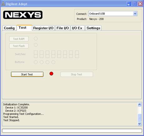
Test your Nexys Board. Using the "Adept" program, open the "Test" tab and click on "Start Test", this loads the demo testing program to the Nexys. This will also erase any programs stored on the Nexys. You can also test the RAM and Flash memory with this utility.