Notes on BJT & FET Transistors.
Comments.
The name transistor comes from the phrase “transferring an electrical signal across a resistor.”
In this course we will discuss two types of transistors:
The Bipolar Junction Transistor (BJT) is an active device. In simple terms, it is a current controlled valve. The base current (IB) controls the collector current (IC).
The Field Effect Transistor (FET) is an active device. In simple terms, it is a voltage controlled valve. The gate-source voltage (VGS) controls the drain current (ID).
Regions of BJT operation:
Cut-off region: The transistor is off. There is no conduction between the collector and the emitter. (IB = 0 therefore IC = 0)
Active region: The transistor is on. The collector current is proportional to and controlled by the base current (IC = βIB) and relatively insensitive to VCE. In this region the transistor can be an amplifier.
Saturation region: The transistor is on. The collector current varies very little with a change in the base current in the saturation region. The VCE is small, a few tenths of a volt. The collector current is strongly dependent on VCE unlike in the active region. It is desirable to operate transistor switches in or near the saturation region when in their on state.
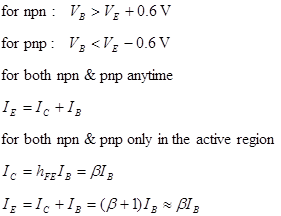
Rules for Bipolar Junction Transistors (BJTs):
- For an npn transistor, the voltage at the collector VC must be greater than the voltage at the emitter VE by at least a few tenths of a volt; otherwise, current will not flow through the collector-emitter junction, no matter what the applied voltage at the base. For pnp transistors, the emitter voltage must be greater than the collector voltage by a similar amount.
- For the npn transistor, there is a voltage drop from the base to the emitter of 0.6 V. For a pnp transistor, there is also a 0.6 V rise from the base to the emitter. In terms of operation, this means that the base voltage VB of an npn transistor must be at least 0.6 V greater that the emitter voltage VE; otherwise, the transistor will not pass emitter-to-collector current. For a pnp transistor, VB must be at least 0.6 V less than VE; otherwise, it will not pass a collector-to-emitter current.
Basic Equations for the BJT.
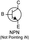
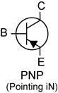
BJT Schematic Symbols (Mnemonics for remembering the direction of the arrows are in parenthesis.)
Ohmmeters view of the BJT. Clearly a transistor cannot be made on the bench by combining two diodes. (Why is that?) Most ohmmeters cannot only measure the resistance, but also measure the forward voltage drop across a diode. From this perspective you can identify the base and the type of transistor based on the following equivalent circuits.


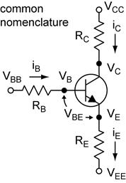
Common Nomenclature (npn example).
Types of Amplifiers.
The transistor is a three terminal device, thus the input and the output must share one terminal in common. This is the origin of the nomenclature of the three types of transistor amplifiers: common collector, common emitter, and common base.
Definition of Gain.
Gain is defined as the ratio of the output signal to the input signal. Because transistor amplifiers often have a quiescent output (a non zero output when the input is zero) we define gain as the derivative of the output with respect to the input. For systems where the quiescent output is zero, this reduces to the ratio of the output to the input. Thus gain is defined as the ratio of the change in output to the change in input.
So far we have not specified the output quantity, the reason is that we can define the gain with respect to any given output and input quantity.
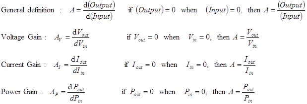
Note that a
negative gain means that the sign of the signal is inverted. Negative gain is
not possible for Power Gain. |A| less than unity indicates that the output is
smaller than the input.
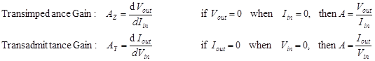
The quantities need not be the same. If the input and output quantities are different, the gain is no longer unitless. The most common examples are transimpedance gain and transadmittance gain.
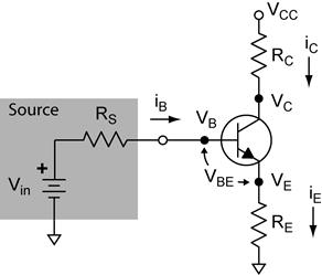
Input Impedance of a Transistor.
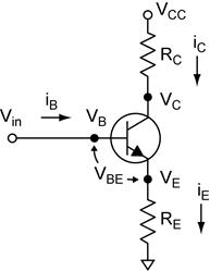
Impedance is defined as Z = V/I. In linear circuits (with resistors, capacitors, inductors, batteries, etc.) this ratio is the reciprocal of the slope of the I versus V graph. In circuits with nonlinear elements such as a transistor, the input impedance of the transistor is defined as the reciprocal of the slope of the I versus V graph. This is simply the derivative of Vin with respect to Iin.
![]()
We can easily find Zin from what we know already of the behavior of the transistor. We know that the sum of VBE and the IR drop across RE must equal Vin.
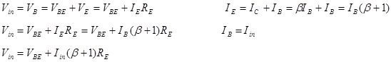
Taking the derivative of Vin with respect to Iin, remembering that VBE is a constant, we get the result:
![]()
![]()
Because IE = IB(β + 1) The IR drop across RE is greater than it would be for IB alone. The amplification of the base current causes RE to appear larger to a source looking into the input by (β + 1).
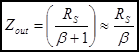
Output Impedance of a Transistor for the Emitter Follower (Common Collector).
The output impedance seen by the load (RE in this example) is defined as:
![]()
The minus sign in the derivative comes from the fact the output impedance has the effect of decreasing Vout. The output current Iout is just the emitter current IE which is related to the base current.
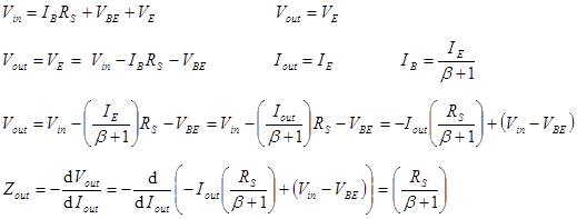
Thus we obtain the result that the impedance of the source, as viewed by the load, is reduced by the factor ~1/β.
The Field Effect Transistor (FET).
The FET is a three terminal device like the BJT, but operates by a different principle. The three terminals are called the source, drain, and gate. The voltage applied to the gate controls the current flowing in the source-drain channel. No current flows through the gate electrode, thus the gate is essentially insulated from the source-drain channel. Because no current flows through the gate, the input impedance of the FET is extremely large (in the range of 1010–1015 Ω). The large input impedance of the FET makes them an excellent choice for amplifier inputs.
The two common families of FETs, the junction FET (JFET) and the metal oxide semiconductor FET (MOSFET) differ in the way the gate contact is made on the source-drain channel.
In the JFET the gate-channel contact is a reverse biased pn junction. The gate-channel junction of the JFET must always be reverse biased otherwise it may behave as a diode. All JFETs are depletion mode devices—they are on when the gate bias is zero (VGS = 0).
In the MOSFET the gate-channel contact is a metal electrode separated from the channel by a thin layer of insulating oxide. MOSFETs have very good isolation between the gate and the channel, but the thin oxide is easily damaged (punctured!) by static discharge through careless handling. MOSFETs are made in both depletion mode (on with zero biased gate, VGS = 0) and in enhancement mode (off with zero biased gate).
In this class we will focus on JFETs.
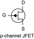
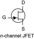
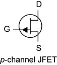
Schematic symbols. Two versions of the symbols are in common use. The symbols in the top row depict the source and drain as being symmetric. This is not generally true. Slight asymmetries are built into the channel during manufacturing which optimize the performance of the FET. Thus it is necessary to distinguish the source from the drain. In this class we will use the asymmetric symbols found on the bottom row, which depict the gate nearly opposite the source. The designation n-channel means that the channel is n doped and the gate is p doped. The p-channel is complement of n-channel.
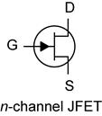
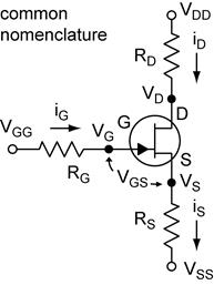
Common Nomenclature (n-channel FET example).
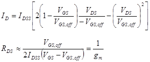
Regions of JFET operation:
Cut-off region: The transistor is off. There is no conduction between the drain and the source when the gate-source voltage is greater than the cut-off voltage. (ID = 0 for VGS > VGS,off)
Active region (also called the Saturation region): The transistor is on. The drain current is controlled by the gate-source voltage (VGS) and relatively insensitive to VDS. In this region the transistor can be an amplifier. IDSS is a parameter that is the maximum drain current, which occurs when the VGS = 0. (The drain current with source shorted to the gate.)
In the active region: 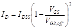
Ohmic region: The transistor is on, but behaves as a voltage controlled resistor. When VDS is less than in the active region, the drain current is roughly proportional to the source-drain voltage and is controlled by the gate voltage.
Common Specifications.
IDSS is the drain current in the active region for VGS = 0. (ID source shorted to gate)
VGS,off is the minimum VGS where ID = 0. VGS,off is negative for n-channel and positive for p-channel..
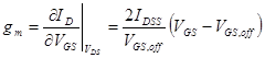
gm is the transconductance, the change in ID with VGS and constant VDS.
Common Circuit Applications:
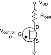
Voltage Controlled Switch. For the on state the gate voltage VGS = 0 and for the off state |VGS| > |VGS,off| (of greater magnitude than VGS,off and with the same sign). The sign of the voltage depends on the type of FET, negative for n-channel and positive for p-channel.
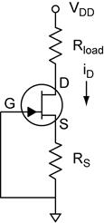
Current Source. The drain current is set by RS such that VGS = −IDRS. Any value of current can be chosen between zero and IDSS (see the ID vs VGS graph for the JFET).
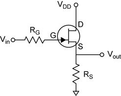
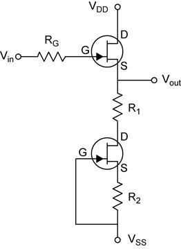
Source Follower. The simple source follower is shown below. The improved version is shown at the right. The lower JFET forms a current source. The result is that VGS is held constant, removing the defects of the simple circuit.
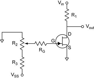
Voltage-Controlled Resistor. VGS must be between zero and VGS,off.
JFET Diode. The JET pn gate junction can be used as a diode by connecting the source and the drain terminals. This is done if very low reverse leakage currents are required. The leakage current is very low because the reverse leakage current scales with the gate area. Small gate areas are designed into JFETs because it decreases the gate-source and the gate-drain capacitances
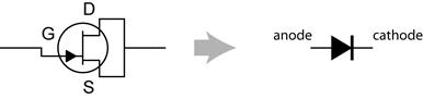 .
.
