Lab 11: JFET: Characteristics and Applications
In this lab you will build 8 different types JFET circuits. You will then use the circuit as an AM transmitter.
In order to do this lab you need to understand the characteristics of JFETs.
Reading Ch 4.3.3+ lecture notes.
Lab credit: Hayes & Horowitz, Student Manual for the Art of Electronics, Cambridge Univ. Press, 1989.
Components:
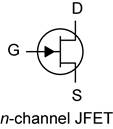
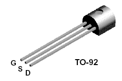
The following circuits use the 2N5485 n-channel JFET in the TO-92
package.
PART 1) FET Characteristics ID vs VGS.
In this part you will measure IDSS, VGS,off,
and ID vs VGS. You will compare your
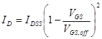
results to the model for the JFET in the active region (AKA saturated region). The
active region model is appropriate in this case because VGS =
15V is large enough to keep the JFET out of the ohmic region (see the ID
vs VDS graphs).
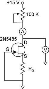
Construct the circuit below. Be sure to choose the DMM with the most sensitive current scale to use as the ammeter. You will need to measure current down to 0.01 μA. The ammeter measures ID. The voltmeter measures VG which is the same as VGS.
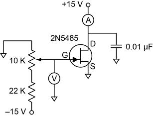
Q 1) 2pts. Why is VG the same as VGS in this circuit?
First check that your circuit works. Use the yellow adjustment tool to operate the potentiometer (variable resistor). At one extreme, VGS = 0 and ID will be a maximum. (The specification sheet for the 2N5485 says that IDSS will fall in the range 4–10 mA.) As you rotate the pot (short for potentiometer) in the other direction, VGS becomes more negative and ID decreases. At some point ID is reduced to zero. Decreasing VGS beyond this point has no further effect.
For these measurements, as you should for any measurements, always use the most sensitive scale available to perform the measurement. For example, do not use the 2 mA scale to measure a 0.1 mA current if a 200 μA scale is available.
Measure IDSS. Adjust the pot so that VGS = 0. Record the current, this is IDSS.
Measure VGS,off. Rotate the pot so that the current is decreasing. When the current just reaches zero on the 20 μA scale, record VGS (use a more sensitive scale if it is available). This is VGS,off. (The specification sheet for the 2N5485 says that VGS,off will fall in the range −0.5 to −4 V.)
Measure ID vs VGS. Make a table in you lab notebook. Make your measurements in the following way. Beginning at VGS,off, increase the current until it reaches approximately 0.3 μA and then record ID and VGS. Continue increasing the current recording data at the approximate ID values of 0.3, 1, 3, 10, 30, 100, 300, 1000, and 3000 μA. Do not waste time setting ID exactly to these values, getting within ~30% of the target value is close enough. What is important is that you measure both the ID and VGS values accurately. You will notice that above 500 μA the voltage points are farther apart. Go back and take a few more data points to fill these gaps. Select voltages within the gaps so that no two points at separated by more than 0.5 V. Add these to you table. Your table should also include IDSS and VGS,off.
Repeat these measurements using you second JFET. Manufacturing variations cause the IDS and VGS,off to vary.
Q 2) 4pts. What are IDSS and VGS,off for each of your JFETs?
Graph 1) 25pts. Graph your data using excel as we did in previous labs. You will graph your experimental data and compare you results to the model. In the plot use open symbols for the experimental points and solid lines for the values calculated from the model. The model is the equation for ID in the active region. The model uses the parameters IDSS and VGS,off that you measured for each JFET. Each JFET must be modeled separately because these parameters will be different. Use different symbols for each set of experimental points and a different line type (e.g. solid or dashed) for the model for each JFET.
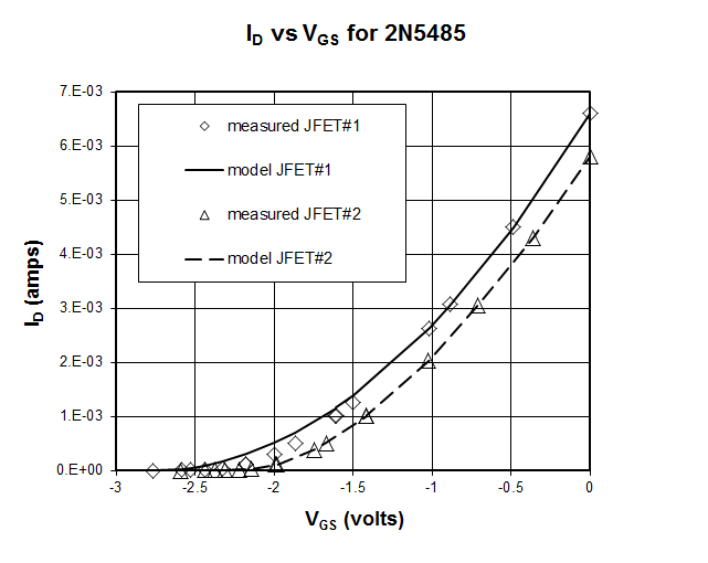
Q 3) 2pts. How closely does your experimental data fit the model?
Before breaking apart this test circuit, you need to make some specific measurements on your JFET for the next part. Measure the VGS where ID = 1.0, 0.5, and 0.1 mA. Do this for each JFET. It’s a fast easy measurement because your have the circuit set up already.
PART 2) FET Current Sources. In part 1 you used an independent voltage source to control VGS. A simple current source can be made from a FET and a source resistor RS. The voltage drop across RS caused by the drain current ID causes the source voltage VS to rise above ground. Grounding VG, this makes VGS negative and acts to reduce ID. The connection between ID and VGS is a simple form of negative feedback. Feedback is the connection between a quantity (ID) and a control (VGS) that acts on that quantity. Negative feedback means that the action of the control (VGS) in response to any change in the quantity (ID), acts to return the quantity (ID) to its equilibrium value. In other words, negative feedback causes the FET to hold ID constant. The value of ID is determined by RS and the ID vs VGS graph.
Make a current source from one of your FETs. You previously measured VGS for ID = 0.1, 0.5, and 1.0 mA. Use these to calculate the value of resistance RS to make VGS = IDRS for each current. Assemble the circuit below using the standard resister values closest to your calculated values of RS.
Q 4) 5pts. Calculate your three resistor values. Show your work. Make a table showing VGS, ID, and RS.
For each of your resistor values, measure the actual resistance. Place the resistor into the circuit as RS. Adjust the pot to give the maximum current; VD should then be nearly 15 V. The pot is the load in this circuit, the device through which you would like to hold the current constant. Rotate the pot to increase its resistance. What happens to ID? What happens to VD?
Q 5) 4pts. When the pot is adjusted to give maximum ID and maximum VD, is the value of the resistance the pot contributes to the circuit a maximum or a minimum?
Q 6) 3pts. For each resistor value make a table of the actual resistor value, the maximum current, and the VD when ID dropped to 90% of its maximum value.
Q 7) 4pts. You have observed the behavior of ID and VD. Generalize your observations and describe what the FET is doing to control the current as you change the resistance of the load (the pot) from one extreme to the other.
PART 3) FET Characteristics ID vs VDS. In this part you will measure ID vs VDS. You will be able to see the active region where ID is essentially independent of VDS and the ohmic region where ID depends strongly on VDS. Construct the circuit shown below. Note that the voltmeter measures VD which in this circuit is the same as VDS.
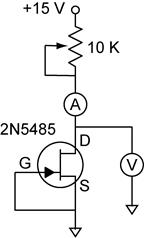
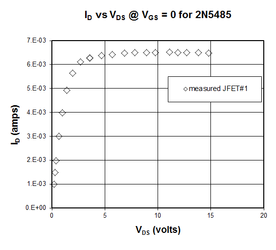
Graph 2) 15pts. Make a table of ID vs VDS. Adjust the pot so that VDS is nearly 15 V. Measure ID and VDS. Adjust the pot to decrease the voltage and record ID and VDS approximately every 2 V until VDS is around 4 V, then take data every 1 V. When ID has dropped ~1 mA below its maximum, begin recording data in approximately 1 mA steps. This procedure will give you an excellent graph with the smallest number of measurements. (See the above example of an excellent graph.)
Q 8) 2pts. How does ID in the active region compare to IDSS that you measured in part 1?
PART 4) FET Source Follower. Construct the circuit below. Connect your function generation to Vin. Set the frequency to 1 kHz and 2 Vp-p. Measure the voltage gain AV = Vout/Vin. (Use peak-to-peak voltages to calculate the gain.)
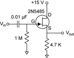
Q 9) 3pts. What is the voltage gain you measured?
Q 10) 4pts. The voltage gain of a follower ideally would be unity. The equation for Vout shows that the gain will be less that unity unless gm is very large. Use the equation for the source follower gain to calculate gm. What is gm for your JFET?
![]()
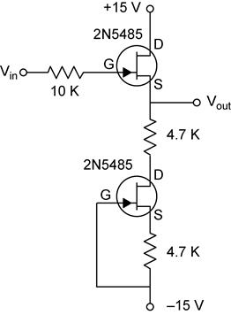
PART 5) Follower with Current-Source Load. The addition of second FET functioning as a current-source load on the upper FET corrects many of the defects of the previous FET source follower circuit. Construct the circuit below. Connect your function generation to Vin. Set the frequency to 1 kHz and 2 Vp-p. Measure the voltage gain AV = Vout/Vin using your oscilloscope. (Use peak-to-peak voltages to calculate the gain.)
Q 11) 3pts. What is the voltage gain you measured?
Q 12) 2pts. The voltage gain of the improved circuit is much closer to unity. Using the equation for the source follower gain, what is the effective value of gm if AV = 1?
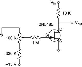
PART 6) The FET as a Variable Resistor. In the ohmic region the FET can be used as a voltage-controlled resistor. In the following circuit the FET forms part of a voltage divider. Construct the circuit below. Connect your function generation to Vin. Set the frequency to 1 kHz and 0.2 Vp-p. Observe Vout using your scope. Adjust the 100K pot. What happens? Measure the min and max Vout/Vin. Is the wave form distorted? Change the waveform to 1 kHz triangle waves and sketch the results at enough different attenuations to describe what is happening.
Q 13) 2pts. What are the min and max Vout/Vin?
Q 14) 6pts. Sketch the shape of the triangle waveforms at enough different attenuations to describe what is happening.
Q 15) 3pts. From your schematic above, calculate the range of VGS spanned by the adjustment. Show how you arrived at your answer.
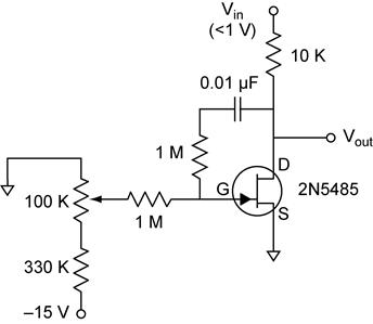
PART 7) Compensated Attenuator. The addition of a resistor and a capacitor improves the voltage controlled attenuator. Repeat the above measurements.
Q 16) 2pts. What are the min and max Vout/Vin?
Q 17) 5pts. Sketch the shape of the triangle waveforms at enough different attenuations to describe what is happening.
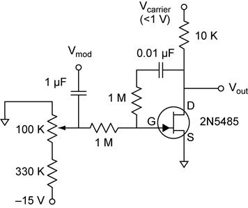
PART 8) AM Modulation: Build your own AM Radio Station. You will need to use both channels of your function generator (FG) for this part. Connect FG CH1 to the Vcarrier input. This is the frequency that will be modulated. Set the carrier frequency to a 20 Vp-p sine wave with a frequency within the AM broadcast band (540-1610 kHz). This is the frequency of your station (and the frequency to which you will need to tune the AM radio). Connect FG CH2 to the Vmod input AND to scope channel 2. Select a modulation tone in the mid audio range 500-5000 Hz and 5 Vp-p amplitude. Vmod controls the amplitude of the carrier wave appearing at Vout. Observe Vout on the oscilloscope channel 1 using the 1 X scope probe.
Scope set up to
view the envelope of the AM modulated wave.
Trigger menu: source = CH2 (Vmod)
Acquire menu: acquisition = peak detect.
Adjust the 100K pot and the amplitudes of the carrier and the modulation. The modulation should not completely pinch off the carrier. Connect a wire ~ 1m long to Vout, this will serve as an antenna. Tune the AM radio through the frequency region of the carrier frequency. When you have found your station, you will hear the modulation tone. Verify that this is in fact your signal by varying the frequency of the tone. Does the tone you hear on the radio change? Adjust the frequency of the carrier. Your station should move on the radio dial. If you change the carrier frequency, you should need to retune your radio to hear your tone again.
Q 18) 4pts. Sketch the envelope of the modulated waveform (Vout) you observe on the scope.