Lab 10: BJT: Characteristics and Applications
In this lab you will build 5 different BJT circuits.
In order to do this lab you need to understand the characteristics of BJTs.
Reading Ch 4.3.1-2+ lecture notes.
Components:
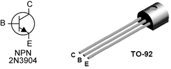
The following circuits use the 2N3904 npn transistor in the TO-92
package.

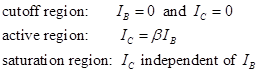
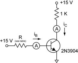
PART 1) BJT Current Amplification Characteristics, IB, IC, and β. In this part you will measure the base current, IB, the collector current, IC, the current amplification, β, and observe their characteristics. You will calculate β, the ratio of IC to IB and graph IC vs IB. For low IB, IC is proportional to IB and only weakly dependent on VCE. This is the active region. For large IB, IC is weakly dependent on IB, but strongly dependent on VCE. This is the saturation region, where we observe that IC levels off. When IB=0, no IC flows, this is the cut-off region, which occurs when VBE < 0.6V.
Construct the circuit below. You will need two DMMs. For each reading, be sure to choose the most sensitive current scale possible on your the DMM. You will need to measure current down to ~1 μA in some cases. Use the resistors in the table below for R to obtain different values of IB. You will use these resistors in Part 2 as well. (Hint: Connect the +15V supply to one of the long buss rows of your breadboard. Insert one lead of all the resistors into that row. Spread them out to make it easier. Then each resistor can then be selected in sequence by attaching the mini-grabber to its other lead.)
|
R |
IB |
IC |
β=IC/IB |
|
|
|
|
|
|
3.3 M |
|
|
|
|
1 M |
|
|
|
|
330 K |
|
|
|
|
100 K |
|
|
|
|
33 K |
|
|
|
|
10 K |
|
|
|
|
3.3 K |
|
|
|
|
1 K |
|
|
|

Graph 1) 8pts. Graph your data using excel as we did in previous labs. (see example graph). This graph should be a log-log plot of log(IC) vs log(IB).
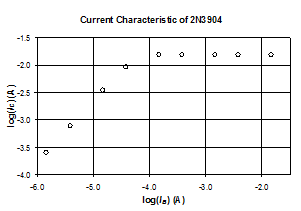
Q 1) 4pts. From your table you can see that β is not constant, but varies with IB. Use your graph to determine which points are in the in the active region. What is the average β for your transistor in the active region?
Q 2) 2pts. If you instead define β as the slope of the IC vs IB graph, what is β in the saturation region?
Q 3) 4pts. What is the maximum IC you measured in the saturation region? If we ignore VCE what is the maximum value of IC?
PART 2) BJT Current Amplification Characteristics, the Darlington pair. The effective current amplification can be increased by connecting two transistors in tandem (Darlington pair). The base current flowing into Q1 is amplified by β1. Q1’s emitter current is connected to Q2’s base, which is again amplified by β2. The overall current gain is β12=β1β2. In our case this is effectively β2 compared to the single transistor.
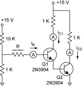
Construct the circuit above. You will need three DMMs. For each reading, be sure to choose the most sensitive current scale possible on your the DMM. You will need to measure current down to 0.01 μA in some cases. Use the resistors in the table below for R to obtain different values of IB. You can use the same resistor set up from Part 1, feeding the input to these resistors with the voltage divider.
|
R |
IB |
IC1 |
IC2 |
β1=IC1/IB |
β12=IC2/IB |
|
10 M |
|
|
|
|
|
|
3.3 M |
|
|
|
|
|
|
1 M |
|
|
|
|
|
|
330 K |
|
|
|
|
|
|
100 K |
|
|
|
|
|
|
33 K |
|
|
|
|
|
|
10 K |
|
|
|
|
|
|
3.3 K |
|
|
|
|
|
|
1 K |
|
|
|
|
|

Graph 2) 14pts. Graph your data using excel as we did in previous labs. (see example graph). This graph should be a log-log plot of log(IC) vs log(IB) showing both the IC1 and IC2 data (see example graph).
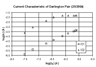
Q 4) 4pts. Compared to the single transistor, has the Darlington pair configuration significantly changed IC2 in the saturation region? Which component is controlling the IC2 saturation current?
Q 5) 6pts. Use your graph to determine which points are in the in the active region for Q1 and for Q2 (these will be different). In their respective active regions, what are the average β for Q1 (IC1/IB) and Q2 (IC2/IB, the Darlington pair β)? From your measurements, is the Darlington pair β approximately the square of the single transistor β?
PART 3) The BJT as a Switch. One of the applications of discrete transistors is that of a switch. Often one needs to control a large current from a small current source. Stated another way, the current gain of the transistor is used to drive a low impedance circuit from a high impedance source.
Construct the circuit shown below. We will drive an LED with your function generator. We will increase impedance of the function generator with the series 10K resistor (shown in the schematic). The LED requires 2-20ma for reasonable brightness. The 2N3904 provides the needed current gain. Drive the input with a <1Hz square wave, use a frequency low enough so you can easily see the LED flashing. Start with a ~10Vp-p square wave. Experiment with the amplitude, DC offset, and waveform.
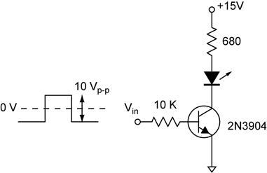
Q 6) 4pts. Measure VCE for the transistor in the on and off states with your DMM. What are these values? Make sure you state which value corresponds to on and off.
Q 7) 2pts. What is the purpose of the 680 Ω resistor?
PART 4) The Emitter Follower. This circuit has unity voltage gain, thus the output voltage follows the input voltage. Although the voltage is not amplified, this circuit will take a “weak” signal from a high impedance source (one that cannot supply much current), and provide a low impedance signal source.
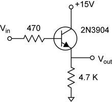
Apply a 5 Vp-p 1 kHz sine wave to Vin. Be sure zero the DC offset of the function generator. Display the input sine wave on channel 1 and observe the output (Vout) in channel 2 using the scope probe.
Q 8) 6pts. Sketch the shape of the waveform you observe in Vout. Also sketch Vin for comparison. Show any clipping or DC offset you observe on the sketch and quantify them by noting the measured voltages on the sketch.
Q 9) 4pts. How does the output waveform compare to the input? Is there a phase shift?
Modify the above circuit to make the circuit below. Connect the emitter resistor to –15V instead common (ground). Note that the circuit no longer shows an explicit connection the common! This is done at the power supply when you configure it as a +15V/–15V source. You will need to connect the function generator common to the power supply common at that point.
Repeat the measurements with this modified circuit.
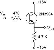
Q 10) 6pts. Sketch the shape of the waveform you observe in Vout. Also sketch Vin for comparison. Show any clipping or DC offset you observe on the sketch and quantify them by noting the measured voltages on the sketch.
Q 11) 4pts. How does the output waveform compare to the input? Is there a phase shift?
Q 12) 4pts. Why is the result different? Explain the salient difference(s).
PART 5) The Common-Emitter Amplifier. Transistor amplifiers are the basis for integrated circuits. In this part you will build a basic common-emitter amplifier which has voltage gain. Build the circuit below and drive it with a 0.3 Vp-p sine wave. Vary the frequency from 1Hz to 1MHz in decade intervals.
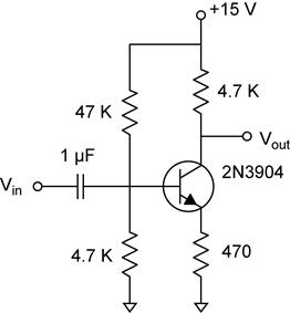
Q 13) 4pts. How do the input and output waveforms compare? Note the salient differences.
Graph 3 and 4) 16pts (8pts ea). Graph the Vp-p vs frequency and phase shift vs frequency. Make sure you have your data table in you notebook!
Q 14) 2pts. What is the voltage gain at 1 kHz? Show the measured Vp-p input and Vp-p output too.
Q 15) 6pts. This circuit contains an RC filter. It is a high-pass or low-pass filter? Which resistors components contribute to the RC filter. What is the corner frequency of this filter?
