
News
Dec 10
Amber Roepe selected for APS Division of Particles and Fields Ethics Advisory Committee
This past summer, the American Physical Society’s (APS) Division of Particles and Fields (DPF) formed the Ethics Advisory Committee (EAC). The...
Mar 25
Physics & Astronomy Offices are Closed
In order to comply with recent public health statements from our Provost, in consultation with OUHSC and the Centers for Disease Control, our departmental offices...
Aug 26
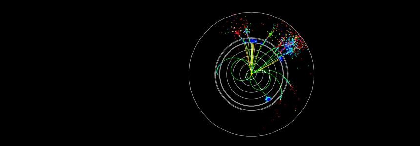
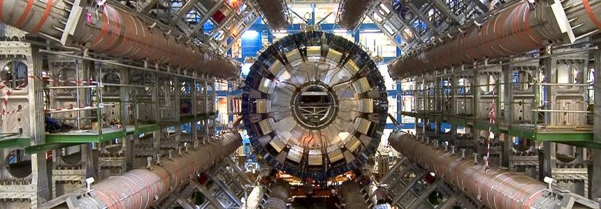
CQRT hiring multiple faculty: applications due by October 20
The Homer L. Dodge Department of Physics and Astronomy at the University of Oklahoma (OU) invites applications for five faculty appointments in the areas of...
Jul 29
Conference for Undergraduate Women in Physics
CUWiP, also known as Conference for Undergraduate Women in Physics, is an annual conference series that has been running since 2006. Since its start, conference participation...

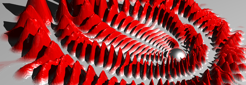
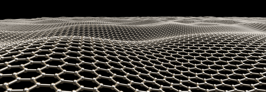
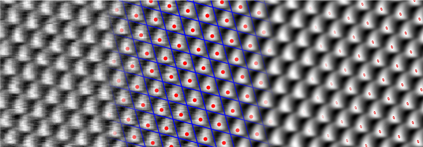
Featured Research: Ferromagnetism with a New Twist
In a new study published in Physical Review Letters, OU postdoc Kangjun Seo and physics professor Bruno Uchoa have found numerical evidence of a novel Mott state that exhibits ferromagnetism at low temperatures. Recent experiments found that when two sheets of graphene are twisted by a very small angle, dubbed a 'magic angle', the combined system behaves as a very strongly correlated system in ways that remind several of the outstanding properties observed in high temperature superconductors.…
